- Record: found
- Abstract: found
- Article: found
Synthesizing a novel genetic sequential logic circuit: a push-on push-off switch
Read this article at
Abstract
-
We designed and constructed a genetic sequential logic circuit that can function as a push-on push-off switch. The circuit consists of a bistable switch module and a NOR gate module.
-
The bistable switch module and NOR gate module were rationally designed and constructed.
-
The two above modules were coupled by two interconnecting parts, cIind- and lacI. When optimizing the defined function, we fine-tuned the expression of the two interconnecting parts by directed evolution.
-
Three control circuits were constructed to show the interconnecting parts are essential for achieving the defined function.
Abstract
Design and synthesis of basic functional circuits are the fundamental tasks of synthetic biologists. Before it is possible to engineer higher-order genetic networks that can perform complex functions, a toolkit of basic devices must be developed. Among those devices, sequential logic circuits are expected to be the foundation of genetic information-processing systems.
As in electronics, combinational and sequential logic circuits are two kinds of fundamental processors in cells. In a combinational logic circuit, the output depends only on the present inputs, whereas in a sequential logic circuit, the output also depends on the history of the input due to its own memory. If we can successfully construct the two kinds of basic logic circuits in a cell, they can serve as building blocks to be assembled into high-order genetic circuits and implement more sophisticated computation.
Construction of genetic combinational logic circuits (GSLCs), such as AND, OR, and NOR gates, has been frequently reported in the last decade ( Guet et al, 2002; Dueber et al, 2003; Anderson et al, 2007; Win and Smolke, 2008). Meanwhile toggle switches, which can function as memory modules, have been implemented in prokaryotic and eukaryotic cells ( Becskei et al, 2001; Kramer et al, 2004; Ajo-Franklin et al, 2007).
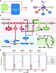
Here, we constructed a novel GSLC that functions as a push-on push-off switch by coupling a combinational logic module with a bistable switch module ( Figure 1A). When the internal state of the memory is in the ‘ON' state, the external UV input makes the circuit's output promoter P NOR generate an ‘OFF' pulse signal and register the ‘OFF' state into the memory; when the internal state is in the ‘OFF' state, the same external UV input induces the circuit's output promoter P NOR to generate an ‘ON' pulse signal and register the ‘ON' state into the memory.
In our design, the combinatorial logic gate is a NOR gate and the switch module is a clearable bistable switch ( Figure 1C). Two interconnecting parts are designed to connect the NOR gate and the bistable switch ( Figure 1D). UV irradiation was used as both an external input signal and a reset signal for the clearable bistable switch ( Figure 1B).
Before implementing the experimental construction, we used a set of ordinary differential equations to simulate the dynamic process. With a set of reasonable parameters, the simulation results showed that the circuit could function as a push-on push-off switch ( Figure 1E). Then the bistable switch module and NOR gate module were rationally designed and constructed. Our experimental results showed that the corresponding functions were implemented very well.
After the construction of the memory and the NOR gate module, we coupled the two modules together by fine-tuning the expression of two interconnecting parts lacI and cI ind− . The two libraries for the ribosome-binding sites (RBSs) of lacI and cI ind− were simultaneously transformed into Escherichia coli cells harboring the memory module plasmid. After growth on agar plates with appropriate antibiotics, colonies containing all three plasmids were selected.
With efficient mutation libraries, we developed a new screening method to select the functional circuits. The experimental process is described in Figure 4A. It consists of two rounds of selection. In the first round of selection, approximatelybout 300 mutants out of 1000 were chosen. In the second round, only three mutants were selected. As shown in Figure 4B, if the initial state was ‘OFF' with green color, the fraction of green cells in the population was near 100% before UV stimulus, whereas less than 10% of cells remained in the green ‘OFF' state after UV stimulus ( Figure 4B). This result indicates that the switch from ‘OFF' to ‘ON' is quite complete. Unfortunately, the switch from ‘ON' to ‘OFF' was not as efficient: only about one-third of the population switched to the ‘OFF' state after UV triggering ( Figure 4C). Nonetheless, the switch is still significant compared with that of the population not exposed to UV irradiation ( Figure 4B and C). These results show that the fine-tuned GSLC can generate different output signals under the same input on the basis of the internal state of its memory, and register the output signal into its memory as the new internal state.
To show that decoupled circuits cannot achieve the sequential logic function, we also constructed three control circuits. The bistable switch module and the NOR gate module were decoupled by removing either or both of the interconnecting parts. In the first control circuit, LacI was removed; without LacI, LexA becomes the only effective input for the NOR gate. As a consequence, upon UV stimulus, promoter P NOR always generates a high output signal, and the ‘ON' state (high CI and low CI434) is latched in the memory with the help of CI ind−. Correspondingly, the color of the cells will change to red. In the other two control circuits, CI ind− or both LacI and CI ind− were removed. Owing to the lack of the feedback part CI ind−, when the output of the promoter P NOR is ‘ON', no output signal can be registered into the memory. In this case, the memory module will spontaneously enter into the low CI/high CI434 state after UV stimulus. All experimental results are consistent with the above expectation.
Finally, to show the property of the push-on push-off switch of the circuit, we sequentially stimulated a homogeneous population of cells with the same dose of UV signal multiple times. The first UV stimulus caused the fraction of green cells in the population to decrease from 99.3% to 8.4%, so that more than 90% of the population switched from the ‘OFF' to the ‘ON' state. The second UV stimulus resulted in the fraction of green cells increasing from 8.4% to 34.5%. Therefore, only 26.1% of the population switched back to the ‘OFF' state. These results are comparable to the results of switching efficiency measurement shown in Figure 4B and C. With repeated exposure to UV irradiation, the population increasingly appeared like a mixture of the two states, the ratio of which gradually reached a steady state. The push-on–push-off function of the circuit was thus lost at the population level.
In summary, we successfully assembled a bistable switch module and a combinatorial NOR gate module into a functional sequential logic circuit. We combined rational design with directed evolution to generate the desired system behavior. In this work, we showed that simultaneous mutation of multiple RBS targets, followed by directed evolution, is a powerful tool to search the in vivo parameter space to generate functional circuits from multiple rationally designed synthetic device modules. We anticipate that this approach will lend itself well to the next step in synthetic biology, combining multiple circuits, each composed of several device modules, to create useful synthetic systems that perform sophisticated computation.
Abstract
Design and synthesis of basic functional circuits are the fundamental tasks of synthetic biologists. Before it is possible to engineer higher-order genetic networks that can perform complex functions, a toolkit of basic devices must be developed. Among those devices, sequential logic circuits are expected to be the foundation of the genetic information-processing systems. In this study, we report the design and construction of a genetic sequential logic circuit in Escherichia coli. It can generate different outputs in response to the same input signal on the basis of its internal state, and ‘memorize' the output. The circuit is composed of two parts: (1) a bistable switch memory module and (2) a double-repressed promoter NOR gate module. The two modules were individually rationally designed, and they were coupled together by fine-tuning the interconnecting parts through directed evolution. After fine-tuning, the circuit could be repeatedly, alternatively triggered by the same input signal; it functions as a push-on push-off switch.
Related collections
Most cited references25
- Record: found
- Abstract: found
- Article: not found
Network motifs in the transcriptional regulation network of Escherichia coli
- Record: found
- Abstract: found
- Article: not found
Self-perpetuating states in signal transduction: positive feedback, double-negative feedback and bistability.
- Record: found
- Abstract: found
- Article: not found