638
views
0
recommends
+1 Recommend
0 collections
    4
    shares
      • Record: found
      • Abstract: found
      • Article: found
      Is Open Access

      Device and circuit-level performance of carbon nanotube field-effect transistor with benchmarking against a nano-MOSFET

      research-article

      Read this article at

      Bookmark
          There is no author summary for this article yet. Authors can add summaries to their articles on ScienceOpen to make them more accessible to a non-specialist audience.

          Abstract

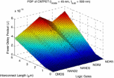
          The performance of a semiconducting carbon nanotube (CNT) is assessed and tabulated for parameters against those of a metal-oxide-semiconductor field-effect transistor (MOSFET). Both CNT and MOSFET models considered agree well with the trends in the available experimental data. The results obtained show that nanotubes can significantly reduce the drain-induced barrier lowering effect and subthreshold swing in silicon channel replacement while sustaining smaller channel area at higher current density. Performance metrics of both devices such as current drive strength, current on-off ratio ( I on/ I off), energy-delay product, and power-delay product for logic gates, namely NAND and NOR, are presented. Design rules used for carbon nanotube field-effect transistors (CNTFETs) are compatible with the 45-nm MOSFET technology. The parasitics associated with interconnects are also incorporated in the model. Interconnects can affect the propagation delay in a CNTFET. Smaller length interconnects result in higher cutoff frequency.

          Related collections

          Most cited references3

          • Record: found
          • Abstract: found
          • Article: found
          Is Open Access

          High-Field, Quasi-Ballistic Transport in Short Carbon Nanotubes

          Single walled carbon nanotubes with Pd ohmic contacts and lengths ranging from several microns down to 10 nm are investigated by electron transport experiments and theory. The mean free path (mfp) for acoustic phonon scattering is estimated to be lap~300 nm, and that for optical phonon scattering is lop~15 nm. Transport through very short (~10 nm) nanotubes is free of significant acoustic and optical phonon scattering and thus ballistic and quasi-ballistic at the low and high bias voltage limits respectively. High currents of up to 70 uA can flow through a short nanotube. Possible mechanisms for the eventual electrical breakdown of short nanotubes at high fields are discussed. The results presented here have important implications to high performance nanotube transistors and interconnects.
            Bookmark
            • Record: found
            • Abstract: found
            • Article: found
            Is Open Access

            High Performance N-Type Carbon Nanotube Field Effect Transistors with Chemically Doped Contacts

            , , (2005)
            Short channel (~80 nm) n-type single-walled carbon nanotube (SWNT) field-effect transistors (FETs) with potassium (K) doped source and drain regions and high-k gate dielectrics (ALD HfO2) are obtained. For nanotubes with diameter ~ 1.6 nm and bandgap ~ 0.55 eV, we obtain n-MOSFET-like devices exhibiting high on-currents due to chemically suppressed Schottky barriers at the contacts, subthreshold swing of 70mV/decade, negligible ambipolar conduction and high on/off ratios up to 10^6 at a bias voltage of 0.5V. The results compare favorably with the state-of-the-art silicon n-MOSFETs and demonstrate the potential of SWNTs for future complementary electronics. The effects of doping level on the electrical characteristics of the nanotube devices are discussed.
              Bookmark
              • Record: found
              • Abstract: found
              • Article: not found

              Multimode transport in Schottky-barrier carbon-nanotube field-effect transistors.

              We present a detailed study on the impact of multimode transport in carbon nanotube field-effect transistors. Under certain field conditions electrical characteristics of tube devices are a result of the contributions of more than one one-dimensional subband. Through potassium doping of the nanotube the impact of the different bands is made visible. We discuss the importance of scattering for a stepwise change of current as a function of gate voltage and explain the implications of our observations for the performance of nanotube transistors.
                Bookmark

                Author and article information

                Journal
                Nanoscale Res Lett
                Nanoscale Res Lett
                Nanoscale Research Letters
                Springer
                1931-7573
                1556-276X
                2012
                19 August 2012
                : 7
                : 1
                : 467
                Affiliations
                [1 ]Faculty of Electrical Engineering, Universiti Teknologi Malaysia, UTM Skudai, Johor, 81310, Malaysia
                [2 ]Electrical Engineering Division, University of Cambridge, 9 J.J. Thomson Ave, Cambridge, CB3 0FA, UK
                Article
                1556-276X-7-467
                10.1186/1556-276X-7-467
                3457859
                22901374
                1b4e90db-7348-4b76-9e8c-08bedddf01bd
                Copyright ©2012 Tan et al.; licensee Springer.

                This is an Open Access article distributed under the terms of the Creative Commons Attribution License ( http://creativecommons.org/licenses/by/2.0), which permits unrestricted use, distribution, and reproduction in any medium, provided the original work is properly cited.

                History
                : 29 June 2012
                : 9 August 2012
                Categories
                Nano Express

                Nanomaterials
                mosfet,device modeling,cntfet,hspice,logic gates,benchmarking
                Nanomaterials
                mosfet, device modeling, cntfet, hspice, logic gates, benchmarking

                Comments

                Comment on this article