22
views
0
recommends
+1 Recommend
0 collections
    0
    shares
      • Record: found
      • Abstract: found
      • Article: not found

      Light-Enhanced Ion Migration in Two-Dimensional Perovskite Single Crystals Revealed in Carbon Nanotubes/Two-Dimensional Perovskite Heterostructure and Its Photomemory Application

      research-article

      Read this article at

      ScienceOpenPublisherPMC
      Bookmark
          There is no author summary for this article yet. Authors can add summaries to their articles on ScienceOpen to make them more accessible to a non-specialist audience.

          Abstract

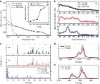
          Two-dimensional (2D) hybrid perovskite sandwiched between two long-chain organic layers is an emerging class of low-cost semiconductor materials with unique optical properties and improved moisture stability. Unlike conventional semiconductors, ion migration in perovskite is a unique phenomenon possibly responsible for long carrier lifetime, current–voltage hysteresis, and low-frequency giant dielectric response. While there are many studies of ion migration in bulk hybrid perovskite, not much is known for its 2D counterparts, especially for ion migration induced by light excitation. Here, we construct an exfoliated 2D perovskite/carbon nanotube (CNT) heterostructure field effect transistor (FET), not only to demonstrate its potential in photomemory applications, but also to study the light induced ion migration mechanisms. We show that the FET IV characteristic curve can be regulated by light and shows two opposite trends under different CNT oxygen doping conditions. Our temperature-dependent study indicates that the change in the IV curve is probably caused by ion redistribution in the 2D hybrid perovskite. The first principle calculation shows the reduction of the migration barrier of I vacancy under light excitation. The device simulation shows that the increase of 2D hybrid perovskite dielectric constant (enabled by the increased ion migration) can change the IV curve in the trends observed experimentally. Finally, the so synthesized FET shows the multilevel photomemory function. Our work shows that not only we could understand the unique ion migration behavior in 2D hybrid perovskite, it might also be used for many future memory function related applications not realizable in traditional semiconductors.

          Abstract

          A two-dimensional perovskite/carbon nanotube heterostructure was constructed not only to study light induced ion migration mechanisms, but also to demonstrate its potential in photomemory applications.

          Related collections

          Most cited references33

          • Record: found
          • Abstract: not found
          • Article: not found

          Generalized Gradient Approximation Made Simple

            Bookmark
            • Record: found
            • Abstract: found
            • Article: not found

            Anomalous Hysteresis in Perovskite Solar Cells.

            Perovskite solar cells have rapidly risen to the forefront of emerging photovoltaic technologies, exhibiting rapidly rising efficiencies. This is likely to continue to rise, but in the development of these solar cells there are unusual characteristics that have arisen, specifically an anomalous hysteresis in the current-voltage curves. We identify this phenomenon and show some examples of factors that make the hysteresis more or less extreme. We also demonstrate stabilized power output under working conditions and suggest that this is a useful parameter to present, alongside the current-voltage scan derived power conversion efficiency. We hypothesize three possible origins of the effect and discuss its implications on device efficiency and future research directions. Understanding and resolving the hysteresis is essential for further progress and is likely to lead to a further step improvement in performance.
              Bookmark
              • Record: found
              • Abstract: found
              • Article: found
              Is Open Access

              One-Year stable perovskite solar cells by 2D/3D interface engineering

              Despite the impressive photovoltaic performances with power conversion efficiency beyond 22%, perovskite solar cells are poorly stable under operation, failing by far the market requirements. Various technological approaches have been proposed to overcome the instability problem, which, while delivering appreciable incremental improvements, are still far from a market-proof solution. Here we show one-year stable perovskite devices by engineering an ultra-stable 2D/3D (HOOC(CH2)4NH3)2PbI4/CH3NH3PbI3 perovskite junction. The 2D/3D forms an exceptional gradually-organized multi-dimensional interface that yields up to 12.9% efficiency in a carbon-based architecture, and 14.6% in standard mesoporous solar cells. To demonstrate the up-scale potential of our technology, we fabricate 10 × 10 cm2 solar modules by a fully printable industrial-scale process, delivering 11.2% efficiency stable for >10,000 h with zero loss in performances measured under controlled standard conditions. This innovative stable and low-cost architecture will enable the timely commercialization of perovskite solar cells.
                Bookmark

                Author and article information

                Journal
                ACS Cent Sci
                ACS Cent Sci
                oc
                acscii
                ACS Central Science
                American Chemical Society
                2374-7943
                2374-7951
                21 October 2019
                27 November 2019
                : 5
                : 11
                : 1857-1865
                Affiliations
                []Institute of Microelectronics, Beijing National Research Center for Information Science and Technology (BNRist), Tsinghua University , Beijing 100084, China
                []Key Laboratory for the Physics and Chemistry of Nanodevices and Department of Electronics, Key Laboratory for the Physics and Chemistry of Nanodevices and College of Chemistry and Molecular Engineering, Peking University , Beijing 100871, China
                [§ ]Material Science Division, Lawrence Berkeley National Laboratory , Berkeley, California, United States
                []School of Optical and Electronic Information, Huazhong University of Science and Technology , Wuhan 430074, China
                Author notes
                [* ](T.-L.R.) E-mail: RenTL@ 123456tsinghua.edu.cn .
                [* ](L.-M.P.) E-mail: lmpeng@ 123456pku.edu.cn .
                [* ](L.-W.W.) E-mail: lwwang@ 123456lbl.gov .
                Article
                10.1021/acscentsci.9b00839
                6891861
                c1b66d16-aff9-4da0-bca2-6d69a443e9d9
                Copyright © 2019 American Chemical Society

                This is an open access article published under an ACS AuthorChoice License, which permits copying and redistribution of the article or any adaptations for non-commercial purposes.

                History
                : 20 August 2019
                Categories
                Research Article
                Custom metadata
                oc9b00839
                oc9b00839

                Comments

                Comment on this article