27
views
0
recommends
+1 Recommend
0 collections
    0
    shares
      • Record: found
      • Abstract: found
      • Article: found
      Is Open Access

      Meniscus-assisted solution printing of large-grained perovskite films for high-efficiency solar cells

      research-article

      Read this article at

      Bookmark
          There is no author summary for this article yet. Authors can add summaries to their articles on ScienceOpen to make them more accessible to a non-specialist audience.

          Abstract

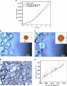
          Control over morphology and crystallinity of metal halide perovskite films is of key importance to enable high-performance optoelectronics. However, this remains particularly challenging for solution-printed devices due to the complex crystallization kinetics of semiconductor materials within dynamic flow of inks. Here we report a simple yet effective meniscus-assisted solution printing (MASP) strategy to yield large-grained dense perovskite film with good crystallization and preferred orientation. Intriguingly, the outward convective flow triggered by fast solvent evaporation at the edge of the meniscus ink imparts the transport of perovskite solutes, thus facilitating the growth of micrometre-scale perovskite grains. The growth kinetics of perovskite crystals is scrutinized by in situ optical microscopy tracking to understand the crystallization mechanism. The perovskite films produced by MASP exhibit excellent optoelectronic properties with efficiencies approaching 20% in planar perovskite solar cells. This robust MASP strategy may in principle be easily extended to craft other solution-printed perovskite-based optoelectronics.

          Abstract

          The morphology control of metal halide perovskite crystalline films is of importance to enable high-performance solar cells. Here, He et al. use a meniscus-assisted solution-based method to print microsized perovskite grains at 60 °C, which results in high optoelectronic device efficiency of 20%.

          Related collections

          Most cited references38

          • Record: found
          • Abstract: found
          • Article: not found

          Solar cells. Impact of microstructure on local carrier lifetime in perovskite solar cells.

          The remarkable performance of hybrid perovskite photovoltaics is attributed to their long carrier lifetimes and high photoluminescence (PL) efficiencies. High-quality films are associated with slower PL decays, and it has been claimed that grain boundaries have a negligible impact on performance. We used confocal fluorescence microscopy correlated with scanning electron microscopy to spatially resolve the PL decay dynamics from films of nonstoichiometric organic-inorganic perovskites, CH3NH3PbI3(Cl). The PL intensities and lifetimes varied between different grains in the same film, even for films that exhibited long bulk lifetimes. The grain boundaries were dimmer and exhibited faster nonradiative decay. Energy-dispersive x-ray spectroscopy showed a positive correlation between chlorine concentration and regions of brighter PL, whereas PL imaging revealed that chemical treatment with pyridine could activate previously dark grains. Copyright © 2015, American Association for the Advancement of Science.
            Bookmark
            • Record: found
            • Abstract: found
            • Article: not found

            Organometallic Halide Perovskites: Sharp Optical Absorption Edge and Its Relation to Photovoltaic Performance.

            Solar cells based on organometallic halide perovskite absorber layers are emerging as a high-performance photovoltaic technology. Using highly sensitive photothermal deflection and photocurrent spectroscopy, we measure the absorption spectrum of CH3NH3PbI3 perovskite thin films at room temperature. We find a high absorption coefficient with particularly sharp onset. Below the bandgap, the absorption is exponential over more than four decades with an Urbach energy as small as 15 meV, which suggests a well-ordered microstructure. No deep states are found down to the detection limit of ∼1 cm(-1). These results confirm the excellent electronic properties of perovskite thin films, enabling the very high open-circuit voltages reported for perovskite solar cells. Following intentional moisture ingress, we find that the absorption at photon energies below 2.4 eV is strongly reduced, pointing to a compositional change of the material.
              Bookmark
              • Record: found
              • Abstract: found
              • Article: not found

              Inkjet printing of single-crystal films.

              The use of single crystals has been fundamental to the development of semiconductor microelectronics and solid-state science. Whether based on inorganic or organic materials, the devices that show the highest performance rely on single-crystal interfaces, with their nearly perfect translational symmetry and exceptionally high chemical purity. Attention has recently been focused on developing simple ways of producing electronic devices by means of printing technologies. 'Printed electronics' is being explored for the manufacture of large-area and flexible electronic devices by the patterned application of functional inks containing soluble or dispersed semiconducting materials. However, because of the strong self-organizing tendency of the deposited materials, the production of semiconducting thin films of high crystallinity (indispensable for realizing high carrier mobility) may be incompatible with conventional printing processes. Here we develop a method that combines the technique of antisolvent crystallization with inkjet printing to produce organic semiconducting thin films of high crystallinity. Specifically, we show that mixing fine droplets of an antisolvent and a solution of an active semiconducting component within a confined area on an amorphous substrate can trigger the controlled formation of exceptionally uniform single-crystal or polycrystalline thin films that grow at the liquid-air interfaces. Using this approach, we have printed single crystals of the organic semiconductor 2,7-dioctyl[1]benzothieno[3,2-b][1]benzothiophene (C(8)-BTBT) (ref. 15), yielding thin-film transistors with average carrier mobilities as high as 16.4 cm(2) V(-1) s(-1). This printing technique constitutes a major step towards the use of high-performance single-crystal semiconductor devices for large-area and flexible electronics applications.
                Bookmark

                Author and article information

                Journal
                Nat Commun
                Nat Commun
                Nature Communications
                Nature Publishing Group
                2041-1723
                07 July 2017
                2017
                : 8
                : 16045
                Affiliations
                [1 ]School of Materials Science and Engineering, Georgia Institute of Technology , Atlanta, Georgia 30332, USA
                [2 ]Laser Dynamics Laboratory, School of Chemistry and Biochemistry, Georgia Institute of Technology , Atlanta, Georgia 30332, USA
                [3 ]Department of Mechanical and Materials Engineering, University of Nebraska–Lincoln , Lincoln, Nebraska 68588, USA
                Author notes
                Author information
                http://orcid.org/0000-0001-9407-9503
                http://orcid.org/0000-0003-3158-9340
                Article
                ncomms16045
                10.1038/ncomms16045
                5504348
                28685751
                08aaaa43-f285-40b8-8955-bb4a436a0b9b
                Copyright © 2017, The Author(s)

                Open Access This article is licensed under a Creative Commons Attribution 4.0 International License, which permits use, sharing, adaptation, distribution and reproduction in any medium or format, as long as you give appropriate credit to the original author(s) and the source, provide a link to the Creative Commons license, and indicate if changes were made. The images or other third party material in this article are included in the article’s Creative Commons license, unless indicated otherwise in a credit line to the material. If material is not included in the article’s Creative Commons license and your intended use is not permitted by statutory regulation or exceeds the permitted use, you will need to obtain permission directly from the copyright holder. To view a copy of this license, visit http://creativecommons.org/licenses/by/4.0/

                History
                : 19 October 2016
                : 23 May 2017
                Categories
                Article

                Uncategorized
                Uncategorized

                Comments

                Comment on this article