17
views
0
recommends
+1 Recommend
0 collections
    0
    shares
      • Record: found
      • Abstract: found
      • Article: found
      Is Open Access

      Recent Progress in Inkjet‐Printed Thin‐Film Transistors

      review-article

      Read this article at

      Bookmark
          There is no author summary for this article yet. Authors can add summaries to their articles on ScienceOpen to make them more accessible to a non-specialist audience.

          Abstract

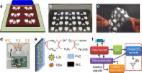
          Drop‐on‐demand inkjet printing is one of the most attractive techniques from a manufacturing perspective due to the possibility of fabrication from a digital layout at ambient conditions, thus leading to great opportunities for the realization of low‐cost and flexible thin‐film devices. Over the past decades, a variety of inkjet‐printed applications including thin‐film transistors (TFTs), radio‐frequency identification devices, sensors, and displays have been explored. In particular, many research groups have made great efforts to realize high‐performance TFTs, for application as potential driving components of ubiquitous wearable electronics. Although there are still challenges to enable the commercialization of printed TFTs beyond laboratory‐scale applications, the field of printed TFTs still attracts significant attention, with remarkable developments in soluble materials and printing methodology. Here, recent progress in printing‐based TFTs is presented from materials to applications. Significant efforts to improve the electrical performance and device‐yield of printed TFTs to match those of counterparts fabricated using conventional deposition or photolithography methods are highlighted. Moreover, emerging low‐dimension printable semiconductors, including carbon nanotubes and transition metal dichalcogenides as well as mature semiconductors, and new‐concept printed switching devices, are also discussed.

          Related collections

          Most cited references55

          • Record: found
          • Abstract: found
          • Article: not found

          Two-dimensional flexible nanoelectronics.

          2014/2015 represents the tenth anniversary of modern graphene research. Over this decade, graphene has proven to be attractive for thin-film transistors owing to its remarkable electronic, optical, mechanical and thermal properties. Even its major drawback--zero bandgap--has resulted in something positive: a resurgence of interest in two-dimensional semiconductors, such as dichalcogenides and buckled nanomaterials with sizeable bandgaps. With the discovery of hexagonal boron nitride as an ideal dielectric, the materials are now in place to advance integrated flexible nanoelectronics, which uniquely take advantage of the unmatched portfolio of properties of two-dimensional crystals, beyond the capability of conventional thin films for ubiquitous flexible systems.
            Bookmark
            • Record: found
            • Abstract: found
            • Article: found
            Is Open Access

            Printable elastic conductors with a high conductivity for electronic textile applications

            The development of advanced flexible large-area electronics such as flexible displays and sensors will thrive on engineered functional ink formulations for printed electronics where the spontaneous arrangement of molecules aids the printing processes. Here we report a printable elastic conductor with a high initial conductivity of 738 S cm−1 and a record high conductivity of 182 S cm−1 when stretched to 215% strain. The elastic conductor ink is comprised of Ag flakes, a fluorine rubber and a fluorine surfactant. The fluorine surfactant constitutes a key component which directs the formation of surface-localized conductive networks in the printed elastic conductor, leading to a high conductivity and stretchability. We demonstrate the feasibility of our inks by fabricating a stretchable organic transistor active matrix on a rubbery stretchability-gradient substrate with unimpaired functionality when stretched to 110%, and a wearable electromyogram sensor printed onto a textile garment.
              Bookmark
              • Record: found
              • Abstract: found
              • Article: found
              Is Open Access

              A wearable chemical–electrophysiological hybrid biosensing system for real-time health and fitness monitoring

              Flexible, wearable sensing devices can yield important information about the underlying physiology of a human subject for applications in real-time health and fitness monitoring. Despite significant progress in the fabrication of flexible biosensors that naturally comply with the epidermis, most designs measure only a small number of physical or electrophysiological parameters, and neglect the rich chemical information available from biomarkers. Here, we introduce a skin-worn wearable hybrid sensing system that offers simultaneous real-time monitoring of a biochemical (lactate) and an electrophysiological signal (electrocardiogram), for more comprehensive fitness monitoring than from physical or electrophysiological sensors alone. The two sensing modalities, comprising a three-electrode amperometric lactate biosensor and a bipolar electrocardiogram sensor, are co-fabricated on a flexible substrate and mounted on the skin. Human experiments reveal that physiochemistry and electrophysiology can be measured simultaneously with negligible cross-talk, enabling a new class of hybrid sensing devices.
                Bookmark

                Author and article information

                Contributors
                seungjun@kist.re.kr
                tlee@snu.ac.kr
                Journal
                Adv Sci (Weinh)
                Adv Sci (Weinh)
                10.1002/(ISSN)2198-3844
                ADVS
                Advanced Science
                John Wiley and Sons Inc. (Hoboken )
                2198-3844
                11 January 2019
                20 March 2019
                : 6
                : 6 ( doiID: 10.1002/advs.v6.6 )
                : 1801445
                Affiliations
                [ 1 ] Photo‐Electronic Hybrids Research Center Korea Institute of Science and Technology Hwarang‐ro 14‐gil 5 Seongbuk‐gu Seoul 02792 South Korea
                [ 2 ] Department of Physics and Astronomy, and Institute of Applied Physics Seoul National University Seoul 08826 South Korea
                Author notes
                Author information
                https://orcid.org/0000-0002-4867-4149
                Article
                ADVS958
                10.1002/advs.201801445
                6425446
                30937255
                2548b141-5a2e-4bd6-9c21-2d5f2023d181
                © 2019 The Authors. Published by WILEY‐VCH Verlag GmbH & Co. KGaA, Weinheim

                This is an open access article under the terms of the http://creativecommons.org/licenses/by/4.0/ License, which permits use, distribution and reproduction in any medium, provided the original work is properly cited.

                History
                : 28 August 2018
                : 25 November 2018
                Page count
                Figures: 26, Tables: 2, Pages: 27, Words: 17398
                Funding
                Funded by: Korea Institute of Science and Technology
                Award ID: 2E28310
                Funded by: National Research Foundation of Korea
                Award ID: NRF‐2017R1C1B2002323
                Funded by: Ministry of Science and ICT of Korea
                Funded by: National Creative Research Laboratory Program
                Award ID: 2012026372
                Categories
                Review
                Reviews
                Custom metadata
                2.0
                advs958
                March 20, 2019
                Converter:WILEY_ML3GV2_TO_NLMPMC version:5.6.1 mode:remove_FC converted:20.03.2019

                flexible devices,inkjet printing,solution processes,switching devices,thin‐film transistors

                Comments

                Comment on this article