20
views
0
recommends
+1 Recommend
0 collections
    0
    shares
      • Record: found
      • Abstract: found
      • Article: found
      Is Open Access

      Biomimetic gyroid nanostructures exceeding their natural origins

      research-article

      Read this article at

      Bookmark
          There is no author summary for this article yet. Authors can add summaries to their articles on ScienceOpen to make them more accessible to a non-specialist audience.

          Abstract

          Researchers demonstrate the replication of 3D natural gyroid nanostructures with superior optical performance and properties.

          Abstract

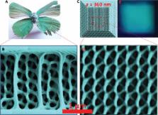
          Using optical two-beam lithography with improved resolution and enhanced mechanical strength, we demonstrate the replication of gyroid photonic nanostructures found in the butterfly Callophrys rubi. These artificial structures are shown to have size, controllability, and uniformity that are superior to those of their biological counterparts. In particular, the elastic Young’s modulus of fabricated nanowires is enhanced by up to 20%. As such, the circular dichroism enabled by the gyroid nanostructures can operate in the near-ultraviolet wavelength region, shorter than that supported by the natural butterfly wings of C. rubi. This fabrication technique provides a unique tool for extracting three-dimensional photonic designs from nature and will aid the investigation of biomimetic nanostructures.

          Related collections

          Most cited references11

          • Record: found
          • Abstract: found
          • Article: not found

          Large-scale synthesis of a silicon photonic crystal with a complete three-dimensional bandgap near 1.5 micrometres

          Photonic technology, using light instead of electrons as the information carrier, is increasingly replacing electronics in communication and information management systems. Microscopic light manipulation, for this purpose, is achievable through photonic bandgap materials, a special class of photonic crystals in which three-dimensional, periodic dielectric constant variations controllably prohibit electromagnetic propagation throughout a specified frequency band. This can result in the localization of photons, thus providing a mechanism for controlling and inhibiting spontaneous light emission that can be exploited for photonic device fabrication. In fact, carefully engineered line defects could act as waveguides connecting photonic devices in all-optical microchips, and infiltration of the photonic material with suitable liquid crystals might produce photonic bandgap structures (and hence light-flow patterns) fully tunable by an externally applied voltage. However, the realization of this technology requires a strategy for the efficient synthesis of high-quality, large-scale photonic crystals with photonic bandgaps at micrometre and sub-micrometre wavelengths, and with rationally designed line and point defects for optical circuitry. Here we describe single crystals of silicon inverse opal with a complete three-dimensional photonic bandgap centred on 1.46 microm, produced by growing silicon inside the voids of an opal template of dose-packed silica spheres that are connected by small 'necks' formed during sintering, followed by removal of the silica template. The synthesis method is simple and inexpensive, yielding photonic crystals of pure silicon that are easily integrated with existing silicon-based microelectronics.
            Bookmark
            • Record: found
            • Abstract: found
            • Article: not found

            On-chip natural assembly of silicon photonic bandgap crystals.

            Photonic bandgap crystals can reflect light for any direction of propagation in specific wavelength ranges. This property, which can be used to confine, manipulate and guide photons, should allow the creation of all-optical integrated circuits. To achieve this goal, conventional semiconductor nanofabrication techniques have been adapted to make photonic crystals. A potentially simpler and cheaper approach for creating three-dimensional periodic structures is the natural assembly of colloidal microspheres. However, this approach yields irregular, polycrystalline photonic crystals that are difficult to incorporate into a device. More importantly, it leads to many structural defects that can destroy the photonic bandgap. Here we show that by assembling a thin layer of colloidal spheres on a silicon substrate, we can obtain planar, single-crystalline silicon photonic crystals that have defect densities sufficiently low that the bandgap survives. As expected from theory, we observe unity reflectance in two crystalline directions of our photonic crystals around a wavelength of 1.3 micrometres. We also show that additional fabrication steps, intentional doping and patterning, can be performed, so demonstrating the potential for specific device applications.
              Bookmark
              • Record: found
              • Abstract: found
              • Article: found
              Is Open Access

              Three-dimensional deep sub-diffraction optical beam lithography with 9 nm feature size.

              The current nanofabrication techniques including electron beam lithography provide fabrication resolution in the nanometre range. The major limitation of these techniques is their incapability of arbitrary three-dimensional nanofabrication. This has stimulated the rapid development of far-field three-dimensional optical beam lithography where a laser beam is focused for maskless direct writing. However, the diffraction nature of light is a barrier for achieving nanometre feature and resolution in optical beam lithography. Here we report on three-dimensional optical beam lithography with 9 nm feature size and 52 nm two-line resolution in a newly developed two-photon absorption resin with high mechanical strength. The revealed dependence of the feature size and the two-line resolution confirms that they can reach deep sub-diffraction scale but are limited by the mechanical strength of the new resin. Our result has paved the way towards portable three-dimensional maskless laser direct writing with resolution fully comparable to electron beam lithography.
                Bookmark

                Author and article information

                Journal
                Sci Adv
                Sci Adv
                SciAdv
                advances
                Science Advances
                American Association for the Advancement of Science
                2375-2548
                May 2016
                13 May 2016
                : 2
                : 5
                : e1600084
                Affiliations
                [1 ]Centre for Micro-Photonics, Faculty of Science, Engineering, and Technology, Swinburne University of Technology, Hawthorn, Victoria 3122, Australia.
                [2 ]Centre for Ultrahigh-bandwidth Devices for Optical Systems (CUDOS), Faculty of Science, Engineering, and Technology, Swinburne University of Technology, Hawthorn, Victoria 3122, Australia.
                [3 ]Artificial-Intelligence Nanophotonics Laboratory, School of Science, RMIT University, Melbourne, Victoria 3001, Australia.
                Author notes
                [* ]Corresponding author. Email: min.gu@ 123456rmit.edu.au
                Article
                1600084
                10.1126/sciadv.1600084
                4928936
                27386542
                7641deeb-85e6-4a32-8540-dbe3b038c665
                Copyright © 2016, The Authors

                This is an open-access article distributed under the terms of the Creative Commons Attribution-NonCommercial license, which permits use, distribution, and reproduction in any medium, so long as the resultant use is not for commercial advantage and provided the original work is properly cited.

                History
                : 17 January 2016
                : 14 April 2016
                Funding
                Funded by: FundRef http://dx.doi.org/10.13039/501100000923, Australian Research Council;
                Award ID: ID0E5EBG6935
                Award ID: Centre for Ultrahigh- bandwidth Devices for Optical Systems (CUDOS) (project number CE110001018)
                Award Recipient :
                Funded by: Laureate Fellowship scheme;
                Award ID: ID0EIOBG6936
                Award ID: FL100100099
                Award Recipient :
                Funded by: FundRef http://dx.doi.org/10.13039/100008716, Science and Industry Endowment Fund;
                Award ID: ID0EQXBG6937
                Award ID: John Stocker Postdoctoral Fellowship (project number PF14-100)
                Award Recipient :
                Categories
                Research Article
                Research Articles
                SciAdv r-articles
                Applied Optics
                Custom metadata
                Meann Ramirez

                gyroid nano-structures,optical two-beam lithography,biomimetics,mechanical strength,circular dichroism

                Comments

                Comment on this article