6
views
0
recommends
+1 Recommend
0 collections
    0
    shares
      • Record: found
      • Abstract: found
      • Article: found
      Is Open Access

      Multi-Level Cell Properties of a Bilayer Cu 2O/Al 2O 3 Resistive Switching Device

      research-article

      Read this article at

      Bookmark
          There is no author summary for this article yet. Authors can add summaries to their articles on ScienceOpen to make them more accessible to a non-specialist audience.

          Abstract

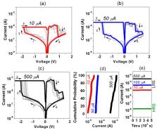
          Multi-level resistive switching characteristics of a Cu 2O/Al 2O 3 bilayer device are presented. An oxidation state gradient in copper oxide induced by the fabrication process was found to play a dominant role in defining the multiple resistance states. The highly conductive grain boundaries of the copper oxide—an unusual property for an oxide semiconductor—are discussed for the first time regarding their role in the resistive switching mechanism.

          Related collections

          Most cited references37

          • Record: found
          • Abstract: not found
          • Article: not found

          High dielectric constant oxides

            Bookmark
            • Record: found
            • Abstract: found
            • Article: not found

            Electrochemical metallization memories--fundamentals, applications, prospects.

            This review focuses on electrochemical metallization memory cells (ECM), highlighting their advantages as the next generation memories. In a brief introduction, the basic switching mechanism of ECM cells is described and the historical development is sketched. In a second part, the full spectra of materials and material combinations used for memory device prototypes and for dedicated studies are presented. In a third part, the specific thermodynamics and kinetics of nanosized electrochemical cells are described. The overlapping of the space charge layers is found to be most relevant for the cell properties at rest. The major factors determining the functionality of the ECM cells are the electrode reaction and the transport kinetics. Depending on electrode and/or electrolyte material electron transfer, electro-crystallization or slow diffusion under strong electric fields can be rate determining. In the fourth part, the major device characteristics of ECM cells are explained. Emphasis is placed on switching speed, forming and SET/RESET voltage, R(ON) to R(OFF) ratio, endurance and retention, and scaling potentials. In the last part, circuit design aspects of ECM arrays are discussed, including the pros and cons of active and passive arrays. In the case of passive arrays, the fundamental sneak path problem is described and as well as a possible solution by two anti-serial (complementary) interconnected resistive switches per cell. Furthermore, the prospects of ECM with regard to further scalability and the ability for multi-bit data storage are addressed.
              Bookmark
              • Record: found
              • Abstract: found
              • Article: not found

              Electrochemical dynamics of nanoscale metallic inclusions in dielectrics.

              Nanoscale metal inclusions in or on solid-state dielectrics are an integral part of modern electrocatalysis, optoelectronics, capacitors, metamaterials and memory devices. The properties of these composite systems strongly depend on the size, dispersion of the inclusions and their chemical stability, and are usually considered constant. Here we demonstrate that nanoscale inclusions (for example, clusters) in dielectrics dynamically change their shape, size and position upon applied electric field. Through systematic in situ transmission electron microscopy studies, we show that fundamental electrochemical processes can lead to universally observed nucleation and growth of metal clusters, even for inert metals like platinum. The clusters exhibit diverse dynamic behaviours governed by kinetic factors including ion mobility and redox rates, leading to different filament growth modes and structures in memristive devices. These findings reveal the microscopic origin behind resistive switching, and also provide general guidance for the design of novel devices involving electronics and ionics.
                Bookmark

                Author and article information

                Journal
                Nanomaterials (Basel)
                Nanomaterials (Basel)
                nanomaterials
                Nanomaterials
                MDPI
                2079-4991
                19 February 2019
                February 2019
                : 9
                : 2
                : 289
                Affiliations
                [1 ]i3N/CENIMAT, Department of Materials Science, Faculty of Science and Technology, Universidade NOVA de Lisboa and CEMOP/UNINOVA, Campus de Caparica, 2829-516 Caparica, Portugal; j.deuermeier@ 123456campus.fct.unl.pt (J.D.); rfpm@ 123456fct.unl.pt (R.M.); emf@ 123456fct.unl.pt (E.F.)
                [2 ]Department of Materials and Earth Sciences, Technische Universität Darmstadt, Otto-Berndt-Straße 3, D-64287 Darmstadt, Germany; aklein@ 123456esm.tu-darmstadt.de
                Author notes
                [* ]Correspondence: a.kiazadeh@ 123456fct.unl.pt ; Tel.: +351212948562
                Author information
                https://orcid.org/0000-0002-2764-3124
                https://orcid.org/0000-0001-7463-1495
                Article
                nanomaterials-09-00289
                10.3390/nano9020289
                6410279
                30791401
                84e99ded-343c-4c9d-ab3a-c8ed0e4e2c71
                © 2019 by the authors.

                Licensee MDPI, Basel, Switzerland. This article is an open access article distributed under the terms and conditions of the Creative Commons Attribution (CC BY) license ( http://creativecommons.org/licenses/by/4.0/).

                History
                : 31 December 2018
                : 14 February 2019
                Categories
                Article

                resistive switching memories,multi-level cell,copper oxide,grain boundaries,aluminum oxide

                Comments

                Comment on this article