6
views
0
recommends
+1 Recommend
0 collections
    0
    shares
      • Record: found
      • Abstract: found
      • Article: found
      Is Open Access

      Van der Waals MoS 2/VO 2 heterostructure junction with tunable rectifier behavior and efficient photoresponse

      research-article

      Read this article at

      Bookmark
          There is no author summary for this article yet. Authors can add summaries to their articles on ScienceOpen to make them more accessible to a non-specialist audience.

          Abstract

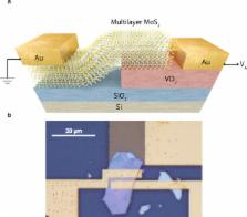
          Junctions between n-type semiconductors of different electron affinity show rectification if the junction is abrupt enough. With the advent of 2D materials, we are able to realize thin van der Waals (vdW) heterostructures based on a large diversity of materials. In parallel, strongly correlated functional oxides have emerged, having the ability to show reversible insulator-to-metal (IMT) phase transition by collapsing their electronic bandgap under a certain external stimulus. Here, we report for the first time the electronic and optoelectronic characterization of ultra-thin n-n heterojunctions fabricated using deterministic assembly of multilayer molybdenum disulphide (MoS 2) on a phase transition material, vanadium dioxide (VO 2). The vdW MoS 2/VO 2 heterojunction combines the excellent blocking capability of an n-n junction with a high conductivity in on-state, and it can be turned into a Schottky rectifier at high applied voltage or at temperatures higher than 68 °C, exploiting the metal state of VO 2. We report tunable diode-like current rectification with a good diode ideality factor of 1.75 and excellent conductance swing of 120 mV/dec. Finally, we demonstrate unique tunable photosensitivity and excellent junction photoresponse in the 500/650 nm wavelength range.

          Related collections

          Most cited references16

          • Record: found
          • Abstract: found
          • Article: found
          Is Open Access

          Growth of Large-Area and Highly Crystalline MoS2 Thin Layers on Insulating Substrates

          The two-dimensional layer of molybdenum disulfide (MoS2) has recently attracted much interest due to its direct-gap property and potential applications in optoelectronics and energy harvesting. However, the synthetic approach to obtain high quality and large-area MoS2 atomic thin layers is still rare. Here we report that the high temperature annealing of a thermally decomposed ammonium thiomolybdate layer in the presence of sulfur can produce large-area MoS2 thin layers with superior electrical performance on insulating substrates. Spectroscopic and microscopic results reveal that the synthesized MoS2 sheets are highly crystalline. The electron mobility of the bottom-gate transistor devices made of the synthesized MoS2 layer is comparable with those of the micromechanically exfoliated thin sheets from MoS2 crystals. This synthetic approach is simple, scalable and applicable to other transition metal dichalcogenides. Meanwhile, the obtained MoS2 films are transferable to arbitrary substrates, providing great opportunities to make layered composites by stacking various atomically thin layers.
            Bookmark
            • Record: found
            • Abstract: found
            • Article: not found

            Ambipolar MoS2 thin flake transistors.

            Field effect transistors (FETs) made of thin flake single crystals isolated from layered materials have attracted growing interest since the success of graphene. Here, we report the fabrication of an electric double layer transistor (EDLT, a FET gated by ionic liquids) using a thin flake of MoS(2), a member of the transition metal dichalcogenides, an archetypal layered material. The EDLT of the thin flake MoS(2) unambiguously displayed ambipolar operation, in contrast to its commonly known bulk property as an n-type semiconductor. High-performance transistor operation characterized by a large "ON" state conductivity in the order of ~mS and a high on/off ratio >10(2) was realized for both hole and electron transport. Hall effect measurements revealed mobility of 44 and 86 cm(2) V(-1) s(-1) for electron and hole, respectively. The hole mobility is twice the value of the electron mobility, and the density of accumulated carrier reached 1 × 10(14) cm(-2), which is 1 order of magnitude larger than conventional FETs with solid dielectrics. The high-density carriers of both holes and electrons can create metallic transport in the MoS(2) channel. The present result is not only important for device applications with new functionalities, but the method itself would also act as a protocol to study this class of material for a broader scope of possibilities in accessing their unexplored properties. © 2012 American Chemical Society
              Bookmark
              • Record: found
              • Abstract: not found
              • Article: not found

              Electrical switching and Mott transition in VO2

                Bookmark

                Author and article information

                Contributors
                nicolo.oliva@epfl.ch
                Journal
                Sci Rep
                Sci Rep
                Scientific Reports
                Nature Publishing Group UK (London )
                2045-2322
                27 October 2017
                27 October 2017
                2017
                : 7
                : 14250
                Affiliations
                [1 ]ISNI 0000000121839049, GRID grid.5333.6, Nanoelectronic Devices Laboratory (NanoLab), École Polytechnique Fédérale de Lausanne (EPFL), ; 1015 Lausanne, Switzerland
                [2 ]ISNI 0000000121839049, GRID grid.5333.6, Nanophotonics and Metrology Laboratory (NAM), École Polytechnique Fédérale de Lausanne (EPFL), ; 1015 Lausanne, Switzerland
                [3 ]ISNI 0000000121839049, GRID grid.5333.6, Solar Energy and Building Physics Laboratory (LESO-PB), École Polytechnique Fédérale de Lausanne (EPFL), ; 1015 Lausanne, Switzerland
                [4 ]ISNI 0000000121839049, GRID grid.5333.6, Istitut de Physique (IPHYS), École Polytechnique Fédérale de Lausanne (EPFL), ; 1015 Lausanne, Switzerland
                Author information
                http://orcid.org/0000-0002-3171-0449
                http://orcid.org/0000-0002-9574-3119
                Article
                12950
                10.1038/s41598-017-12950-y
                5660225
                29079744
                bd519a21-627a-43fe-a944-a12add465460
                © The Author(s) 2017

                Open Access This article is licensed under a Creative Commons Attribution 4.0 International License, which permits use, sharing, adaptation, distribution and reproduction in any medium or format, as long as you give appropriate credit to the original author(s) and the source, provide a link to the Creative Commons license, and indicate if changes were made. The images or other third party material in this article are included in the article’s Creative Commons license, unless indicated otherwise in a credit line to the material. If material is not included in the article’s Creative Commons license and your intended use is not permitted by statutory regulation or exceeds the permitted use, you will need to obtain permission directly from the copyright holder. To view a copy of this license, visit http://creativecommons.org/licenses/by/4.0/.

                History
                : 6 June 2017
                : 12 September 2017
                Categories
                Article
                Custom metadata
                © The Author(s) 2017

                Uncategorized
                Uncategorized

                Comments

                Comment on this article