41
views
0
recommends
+1 Recommend
0 collections
    0
    shares
      • Record: found
      • Abstract: found
      • Article: found
      Is Open Access

      Direct oriented growth of armchair graphene nanoribbons on germanium

      research-article

      Read this article at

      Bookmark
          There is no author summary for this article yet. Authors can add summaries to their articles on ScienceOpen to make them more accessible to a non-specialist audience.

          Abstract

          Graphene can be transformed from a semimetal into a semiconductor if it is confined into nanoribbons narrower than 10 nm with controlled crystallographic orientation and well-defined armchair edges. However, the scalable synthesis of nanoribbons with this precision directly on insulating or semiconducting substrates has not been possible. Here we demonstrate the synthesis of graphene nanoribbons on Ge(001) via chemical vapour deposition. The nanoribbons are self-aligning 3° from the Ge〈110〉 directions, are self-defining with predominantly smooth armchair edges, and have tunable width to <10 nm and aspect ratio to >70. In order to realize highly anisotropic ribbons, it is critical to operate in a regime in which the growth rate in the width direction is especially slow, <5 nm h −1. This directional and anisotropic growth enables nanoribbon fabrication directly on conventional semiconductor wafer platforms and, therefore, promises to allow the integration of nanoribbons into future hybrid integrated circuits.

          Abstract
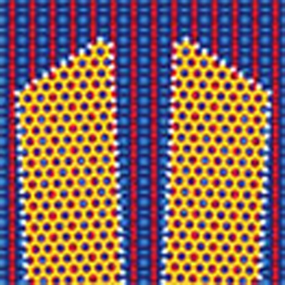
          Semiconducting armchair graphene nanoribbons with sub-10 nm width are of great technological importance but yet to realize. Here, the authors report growth of such nanoribbons on germanium and controlled crystallographic orientation and well-defined armchair edges are obtained.

          Related collections

          Most cited references64

          • Record: found
          • Abstract: found
          • Article: found
          Is Open Access

          Half-Metallic Graphene Nanoribbons

          Electrical current can be completely spin polarized in a class of materials known as half-metals, as a result of the coexistence of metallic nature for electrons with one spin orientation and insulating for electrons with the other. Such asymmetric electronic states for the different spins have been predicted for some ferromagnetic metals - for example, the Heusler compounds- and were first observed in a manganese perovskite. In view of the potential for use of this property in realizing spin-based electronics, substantial efforts have been made to search for half-metallic materials. However, organic materials have hardly been investigated in this context even though carbon-based nanostructures hold significant promise for future electronic device. Here we predict half-metallicity in nanometre-scale graphene ribbons by using first-principles calculations. We show that this phenomenon is realizable if in-plane homogeneous electric fields are applied across the zigzag-shaped edges of the graphene nanoribbons, and that their magnetic property can be controlled by the external electric fields. The results are not only of scientific interests in the interplay between electric fields and electronic spin degree of freedom in solids but may also open a new path to explore spintronics at nanometre scale, based on graphene.
            Bookmark
            • Record: found
            • Abstract: found
            • Article: found
            Is Open Access

            Energy Band Gap Engineering of Graphene Nanoribbons

            We investigate electronic transport in lithographically patterned graphene ribbon structures where the lateral confinement of charge carriers creates an energy gap near the charge neutrality point. Individual graphene layers are contacted with metal electrodes and patterned into ribbons of varying widths and different crystallographic orientations. The temperature dependent conductance measurements show larger energy gaps opening for narrower ribbons. The sizes of these energy gaps are investigated by measuring the conductance in the non-linear response regime at low temperatures. We find that the energy gap scales inversely with the ribbon width, thus demonstrating the ability to engineer the band gap of graphene nanostructures by lithographic processes.
              Bookmark
              • Record: found
              • Abstract: found
              • Article: not found

              Half-metallic graphene nanoribbons.

              Electrical current can be completely spin polarized in a class of materials known as half-metals, as a result of the coexistence of metallic nature for electrons with one spin orientation and insulating nature for electrons with the other. Such asymmetric electronic states for the different spins have been predicted for some ferromagnetic metals--for example, the Heusler compounds--and were first observed in a manganese perovskite. In view of the potential for use of this property in realizing spin-based electronics, substantial efforts have been made to search for half-metallic materials. However, organic materials have hardly been investigated in this context even though carbon-based nanostructures hold significant promise for future electronic devices. Here we predict half-metallicity in nanometre-scale graphene ribbons by using first-principles calculations. We show that this phenomenon is realizable if in-plane homogeneous electric fields are applied across the zigzag-shaped edges of the graphene nanoribbons, and that their magnetic properties can be controlled by the external electric fields. The results are not only of scientific interest in the interplay between electric fields and electronic spin degree of freedom in solids but may also open a new path to explore spintronics at the nanometre scale, based on graphene.
                Bookmark

                Author and article information

                Journal
                Nat Commun
                Nat Commun
                Nature Communications
                Nature Publishing Group
                2041-1723
                10 August 2015
                2015
                : 6
                : 8006
                Affiliations
                [1 ]Department of Materials Science and Engineering, University of Wisconsin-Madison , Madison, Wisconsin 53706, USA
                [2 ]Center for Nanoscale Materials, Argonne National Laboratory , Argonne, Illinois 60439, USA
                [3 ]Department of Materials Science and Engineering, Northwestern University , Evanston, Illinois 60208, USA
                [4 ]Department of Engineering Physics, École Polytechnique de Montréal , Montréal, Québec, Canada H3C 2A7
                [5 ]Department of Chemistry, Université de Montréal , Montréal, Québec, Canada H3C 3JT
                [6 ]Department of Chemistry, Northwestern University , Evanston, Illinois 60208, USA
                Author notes
                Author information
                http://orcid.org/0000-0003-0421-6792
                http://orcid.org/0000-0002-9021-4656
                Article
                ncomms9006
                10.1038/ncomms9006
                4918381
                26258594
                28548339-46f0-48b2-b069-d1894f34fec8
                Copyright © 2015, Nature Publishing Group, a division of Macmillan Publishers Limited. All Rights Reserved.

                This work is licensed under a Creative Commons Attribution 4.0 International License. The images or other third party material in this article are included in the article's Creative Commons license, unless indicated otherwise in the credit line; if the material is not included under the Creative Commons license, users will need to obtain permission from the license holder to reproduce the material. To view a copy of this license, visit http://creativecommons.org/licenses/by/4.0/

                History
                : 25 January 2015
                : 03 July 2015
                Categories
                Article

                Uncategorized
                Uncategorized

                Comments

                Comment on this article