5
views
0
recommends
+1 Recommend
0 collections
    0
    shares
      • Record: found
      • Abstract: found
      • Article: found
      Is Open Access

      Scalable high performance radio frequency electronics based on large domain bilayer MoS 2

      research-article

      Read this article at

      Bookmark
          There is no author summary for this article yet. Authors can add summaries to their articles on ScienceOpen to make them more accessible to a non-specialist audience.

          Abstract

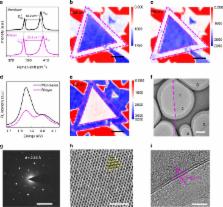
          Atomically-thin layered molybdenum disulfide (MoS 2) has attracted tremendous research attention for their potential applications in high performance DC and radio frequency electronics, especially for flexible electronics. Bilayer MoS 2 is expected to have higher electron mobility and higher density of states with higher performance compared with single layer MoS 2. Here, we systematically investigate the synthesis of high quality bilayer MoS 2 by chemical vapor deposition on molten glass with increasing domain sizes up to 200 μm. High performance transistors with optimized high- κ dielectrics deliver ON-current of 427 μA μm −1 at 300 K and a record high ON-current of 1.52 mA μm −1 at 4.3 K. Moreover, radio frequency transistors are demonstrated with an extrinsic high cut-off frequency of 7.2 GHz and record high extrinsic maximum frequency of oscillation of 23 GHz, together with gigahertz MoS 2 mixers on flexible polyimide substrate, showing the great potential for future high performance DC and high-frequency electronics.

          Abstract

          Large area two-dimensional materials show promise for applications in DC and RF flexible electronics. Here, the authors report RF transistors based on chemical vapor deposited bilayer MoS 2 with 23 GHz extrinsic maximum oscillation frequency, and gigahertz mixers on flexible polyimide substrates.

          Related collections

          Most cited references47

          • Record: found
          • Abstract: found
          • Article: not found

          Emerging photoluminescence in monolayer MoS2.

          Novel physical phenomena can emerge in low-dimensional nanomaterials. Bulk MoS(2), a prototypical metal dichalcogenide, is an indirect bandgap semiconductor with negligible photoluminescence. When the MoS(2) crystal is thinned to monolayer, however, a strong photoluminescence emerges, indicating an indirect to direct bandgap transition in this d-electron system. This observation shows that quantum confinement in layered d-electron materials like MoS(2) provides new opportunities for engineering the electronic structure of matter at the nanoscale.
            Bookmark
            • Record: found
            • Abstract: found
            • Article: not found

            High-mobility three-atom-thick semiconducting films with wafer-scale homogeneity.

            The large-scale growth of semiconducting thin films forms the basis of modern electronics and optoelectronics. A decrease in film thickness to the ultimate limit of the atomic, sub-nanometre length scale, a difficult limit for traditional semiconductors (such as Si and GaAs), would bring wide benefits for applications in ultrathin and flexible electronics, photovoltaics and display technology. For this, transition-metal dichalcogenides (TMDs), which can form stable three-atom-thick monolayers, provide ideal semiconducting materials with high electrical carrier mobility, and their large-scale growth on insulating substrates would enable the batch fabrication of atomically thin high-performance transistors and photodetectors on a technologically relevant scale without film transfer. In addition, their unique electronic band structures provide novel ways of enhancing the functionalities of such devices, including the large excitonic effect, bandgap modulation, indirect-to-direct bandgap transition, piezoelectricity and valleytronics. However, the large-scale growth of monolayer TMD films with spatial homogeneity and high electrical performance remains an unsolved challenge. Here we report the preparation of high-mobility 4-inch wafer-scale films of monolayer molybdenum disulphide (MoS2) and tungsten disulphide, grown directly on insulating SiO2 substrates, with excellent spatial homogeneity over the entire films. They are grown with a newly developed, metal-organic chemical vapour deposition technique, and show high electrical performance, including an electron mobility of 30 cm(2) V(-1) s(-1) at room temperature and 114 cm(2) V(-1) s(-1) at 90 K for MoS2, with little dependence on position or channel length. With the use of these films we successfully demonstrate the wafer-scale batch fabrication of high-performance monolayer MoS2 field-effect transistors with a 99% device yield and the multi-level fabrication of vertically stacked transistor devices for three-dimensional circuitry. Our work is a step towards the realization of atomically thin integrated circuitry.
              Bookmark
              • Record: found
              • Abstract: found
              • Article: not found

              Large-area vapor-phase growth and characterization of MoS(2) atomic layers on a SiO(2) substrate.

              Atomic-layered MoS(2) is synthesized directly on SiO(2) substrates by a scalable chemical vapor deposition method. The large-scale synthesis of an atomic-layered semiconductor directly on a dielectric layer paves the way for many facile device fabrication possibilities, expanding the important family of useful mono- or few-layer materials that possess exceptional properties, such as graphene and hexagonal boron nitride (h-BN). Copyright © 2012 WILEY-VCH Verlag GmbH & Co. KGaA, Weinheim.
                Bookmark

                Author and article information

                Contributors
                yqwu@mail.hust.edu.cn
                Journal
                Nat Commun
                Nat Commun
                Nature Communications
                Nature Publishing Group UK (London )
                2041-1723
                14 November 2018
                14 November 2018
                2018
                : 9
                : 4778
                Affiliations
                ISNI 0000 0004 0368 7223, GRID grid.33199.31, Wuhan National High Magnetic Field Center and School of Optical and Electronic Information, , Huazhong University of Science and Technology, ; Wuhan, 430074 China
                Author information
                http://orcid.org/0000-0003-2578-5214
                Article
                7135
                10.1038/s41467-018-07135-8
                6235828
                30429471
                340fd22f-5721-4ec1-8169-93e5f09f241d
                © The Author(s) 2018

                Open Access This article is licensed under a Creative Commons Attribution 4.0 International License, which permits use, sharing, adaptation, distribution and reproduction in any medium or format, as long as you give appropriate credit to the original author(s) and the source, provide a link to the Creative Commons license, and indicate if changes were made. The images or other third party material in this article are included in the article’s Creative Commons license, unless indicated otherwise in a credit line to the material. If material is not included in the article’s Creative Commons license and your intended use is not permitted by statutory regulation or exceeds the permitted use, you will need to obtain permission directly from the copyright holder. To view a copy of this license, visit http://creativecommons.org/licenses/by/4.0/.

                History
                : 27 March 2018
                : 15 October 2018
                Categories
                Article
                Custom metadata
                © The Author(s) 2018

                Uncategorized
                Uncategorized

                Comments

                Comment on this article