- Record: found
- Abstract: found
- Article: found
Effect of film thickness and evaporation rate on co-evaporated SnSe thin films for photovoltaic applications

Read this article at
Abstract
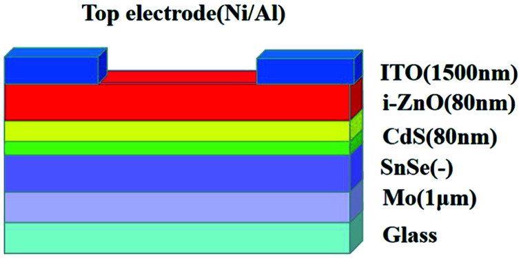
SnSe thin films were deposited by a co-evaporation method with different film thicknesses and evaporation rates. A device with a structure of soda-lime glass/Mo/SnSe/CdS/i-ZnO/ITO/Ni/Al was fabricated. Device efficiency was improved from 0.18% to 1.02% by a film thickness of 1.3 μm and evaporation rate of 2.5 Å S −1 via augmentation of short-circuit current density and open-circuit voltage. Properties (electrical, optical, structural) and scanning electron microscopy measurements were compared for samples. A SnSe thin-film solar cell prepared with a film thickness of 1.3 μm and evaporation rate of 2.5 Å S −1 had the highest electron mobility, better crystalline properties, and larger grain size compared with the other solar cells prepared. These data can be used to guide growth of high-quality SnSe thin films, and contribute to development of efficient SnSe thin-film solar cells using an evaporation-based method.
Abstract
SnSe thin films were deposited by a co-evaporation method with different film thicknesses and evaporation rates.
Related collections
Most cited references28

- Record: found
- Abstract: found
- Article: found
Tin Selenide (SnSe): Growth, Properties, and Applications
- Record: found
- Abstract: found
- Article: not found
Structure and electronic properties of grain boundaries in earth-abundant photovoltaic absorber Cu2ZnSnSe4.
- Record: found
- Abstract: not found
- Article: not found