1
views
0
recommends
+1 Recommend
0 collections
    0
    shares
      • Record: found
      • Abstract: found
      • Article: found
      Is Open Access

      Field Emission Characterization of MoS 2 Nanoflowers
      research-article

      Read this article at

      Bookmark
          There is no author summary for this article yet. Authors can add summaries to their articles on ScienceOpen to make them more accessible to a non-specialist audience.

          Abstract

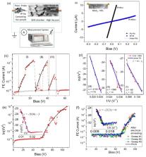
          Nanostructured materials have wide potential applicability as field emitters due to their high aspect ratio. We hydrothermally synthesized MoS 2 nanoflowers on copper foil and characterized their field emission properties, by applying a tip-anode configuration in which a tungsten tip with curvature radius down to 30–100 nm has been used as the anode to measure local properties from small areas down to 1–100 µm 2. We demonstrate that MoS 2 nanoflowers can be competitive with other well-established field emitters. Indeed, we show that a stable field emission current can be measured with a turn-on field as low as 12 V/μm and a field enhancement factor up to 880 at 0.6 μm cathode–anode separation distance.

          Related collections

          Most cited references62

          • Record: found
          • Abstract: found
          • Article: not found

          Graphene-MoS2 hybrid structures for multifunctional photoresponsive memory devices.

          Combining the electronic properties of graphene and molybdenum disulphide (MoS2) in hybrid heterostructures offers the possibility to create devices with various functionalities. Electronic logic and memory devices have already been constructed from graphene-MoS2 hybrids, but they do not make use of the photosensitivity of MoS2, which arises from its optical-range bandgap. Here, we demonstrate that graphene-on-MoS2 binary heterostructures display remarkable dual optoelectronic functionality, including highly sensitive photodetection and gate-tunable persistent photoconductivity. The responsivity of the hybrids was found to be nearly 1 × 10(10) A W(-1) at 130 K and 5 × 10(8) A W(-1) at room temperature, making them the most sensitive graphene-based photodetectors. When subjected to time-dependent photoillumination, the hybrids could also function as a rewritable optoelectronic switch or memory, where the persistent state shows almost no relaxation or decay within experimental timescales, indicating near-perfect charge retention. These effects can be quantitatively explained by gate-tunable charge exchange between the graphene and MoS2 layers, and may lead to new graphene-based optoelectronic devices that are naturally scalable for large-area applications at room temperature.
            Bookmark
            • Record: found
            • Abstract: found
            • Article: not found

            Sensing behavior of atomically thin-layered MoS2 transistors.

            Most of recent research on layered chalcogenides is understandably focused on single atomic layers. However, it is unclear if single-layer units are the most ideal structures for enhanced gas-solid interactions. To probe this issue further, we have prepared large-area MoS2 sheets ranging from single to multiple layers on 300 nm SiO2/Si substrates using the micromechanical exfoliation method. The thickness and layering of the sheets were identified by optical microscope, invoking recently reported specific optical color contrast, and further confirmed by AFM and Raman spectroscopy. The MoS2 transistors with different thicknesses were assessed for gas-sensing performances with exposure to NO2, NH3, and humidity in different conditions such as gate bias and light irradiation. The results show that, compared to the single-layer counterpart, transistors of few MoS2 layers exhibit excellent sensitivity, recovery, and ability to be manipulated by gate bias and green light. Further, our ab initio DFT calculations on single-layer and bilayer MoS2 show that the charge transfer is the reason for the decrease in resistance in the presence of applied field.
              Bookmark
              • Record: found
              • Abstract: not found
              • Article: not found

              Thermionic Emission, Field Emission, and the Transition Region

                Bookmark

                Author and article information

                Journal
                Nanomaterials (Basel)
                Nanomaterials (Basel)
                nanomaterials
                Nanomaterials
                MDPI
                2079-4991
                09 May 2019
                May 2019
                : 9
                : 5
                : 717
                Affiliations
                [1 ]CNR-SPIN Salerno, via Giovanni Paolo II n. 132, 84084 Fisciano, Italy; furban@ 123456unisa.it (F.U.); liemmo@ 123456unisa.it (L.I.); giluongo@ 123456unisa.it (G.L.)
                [2 ]Physics Department “E. R. Caianiello”, University of Salerno, via Giovanni Paolo II n. 132, 84084 Fisciano, Italy; agrillo@ 123456unisa.it (A.G.); aniello.pelella@ 123456gmail.com (A.P.)
                [3 ]Department of Physical and Chemical Science, University of L’Aquila, via Vetoio, Coppito, 67100 L’Aquila, Italy; mpassac@ 123456aquila.infn.it (M.P.); luca.lozzi@ 123456aquila.infn.it (L.L.)
                [4 ]WMG, International Manufacturing Centre, University of Warwick, Coventry CV4 7AL, UK; M.Loveridge@ 123456warwick.ac.uk
                Author notes
                Author information
                https://orcid.org/0000-0003-2233-3810
                https://orcid.org/0000-0002-8909-9865
                https://orcid.org/0000-0002-3680-5295
                https://orcid.org/0000-0003-2109-1370
                https://orcid.org/0000-0002-5111-3887
                https://orcid.org/0000-0002-9071-2647
                https://orcid.org/0000-0003-2908-3885
                https://orcid.org/0000-0002-3629-726X
                Article
                nanomaterials-09-00717
                10.3390/nano9050717
                6566819
                31075873
                52317bd9-eaa8-4a41-9a52-d2c30ad53f7d
                © 2019 by the authors.

                Licensee MDPI, Basel, Switzerland. This article is an open access article distributed under the terms and conditions of the Creative Commons Attribution (CC BY) license ( http://creativecommons.org/licenses/by/4.0/).

                History
                : 05 April 2019
                : 06 May 2019
                Categories
                Article

                transition metal dichalcogenides,mos2,nanoflower,field emission

                Comments

                Comment on this article