1
views
0
recommends
+1 Recommend
0 collections
    0
    shares
      • Record: found
      • Abstract: found
      • Article: found
      Is Open Access

      Room-temperature liquid diffused separation induced crystallization for high-quality perovskite single crystals

      research-article

      Read this article at

      Bookmark
          There is no author summary for this article yet. Authors can add summaries to their articles on ScienceOpen to make them more accessible to a non-specialist audience.

          Abstract

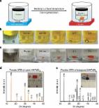
          Large single crystals serve as an ideal platform for investigating intrinsic material properties and optoelectronic applications. Here we develop a method, namely, room-temperature liquid diffused separation induced crystallization that uses silicone oil to separate the solvent from the perovskite precursors, to grow high-quality perovskite single crystals. The growth kinetics of perovskite single crystals using this method is elucidated, and their structural and optoelectronic properties are carefully characterized. The resultant perovskite single crystals, taking CH 3NH 3PbBr 3 as an example, exhibit approximately 1 µs lifetime, a low trap density of 4.4 × 10 9 cm −3, and high yield of 92%, which are appealing for visible light or X-ray detection. We hope our findings will be of great significance for the continued advancement of high-quality perovskite single crystals, through a better understanding of growth mechanisms and their deployment in various optoelectronics. The diffused separation induced crystallization strategy presents a major step forward for advancing the field on perovskite single crystals.

          Abstract

          Perovskites are appealing for optoelectronics, but high-quality perovskite single crystals should be grown at low temperature to minimize trap density. Here, the authors report a room-temperature liquid-diffused-induced crystallization for growth of high-quality hybrid perovskite single crystals.

          Related collections

          Most cited references45
          • Record: found
          • Abstract: found
          • Article: found
          Is Open Access

          High-quality bulk hybrid perovskite single crystals within minutes by inverse temperature crystallization

          Single crystals of methylammonium lead trihalide perovskites (MAPbX3; MA=CH3NH3 +, X=Br− or I−) have shown remarkably low trap density and charge transport properties; however, growth of such high-quality semiconductors is a time-consuming process. Here we present a rapid crystal growth process to obtain MAPbX3 single crystals, an order of magnitude faster than previous reports. The process is based on our observation of the substantial decrease of MAPbX3 solubility, in certain solvents, at elevated temperatures. The crystals can be both size- and shape-controlled by manipulating the different crystallization parameters. Despite the rapidity of the method, the grown crystals exhibit transport properties and trap densities comparable to the highest quality MAPbX3 reported to date. The phenomenon of inverse or retrograde solubility and its correlated inverse temperature crystallization strategy present a major step forward for advancing the field on perovskite crystallization.
            Bookmark
            • Record: found
            • Abstract: found
            • Article: not found

            Two-Inch-Sized Perovskite CH3 NH3 PbX3 (X = Cl, Br, I) Crystals: Growth and Characterization.

            Two-inch-sized perovskite crystals, CH3 NH3 PbX3 (X=I, Br, Cl), with high crystalline quality are prepared by a solution-grown strategy. The availability of large perovskite crystals is expected to transform its broad applications in photovoltaics, optoelectronics, lasers, photodetectors, LEDs, etc., just as crystalline silicon has done in revolutionizing the modern electronics and photovoltaic industries.
              Bookmark
              • Record: found
              • Abstract: found
              • Article: not found

              Printable organometallic perovskite enables large-area, low-dose X-ray imaging

              Medical X-ray imaging procedures require digital flat detectors operating at low doses to reduce radiation health risks. Solution-processed organic–inorganic hybrid perovskites have characteristics that make them good candidates for the photoconductive layer of such sensitive detectors. However, such detectors have not yet been built on thin-film transistor arrays because it has been difficult to prepare thick perovskite films (more than a few hundred micrometres) over large areas (a detector is typically 50 centimetres by 50 centimetres). We report here an all-solution-based (in contrast to conventional vacuum processing) synthetic route to producing printable polycrystalline perovskites with sharply faceted large grains having morphologies and optoelectronic properties comparable to those of single crystals. High sensitivities of up to 11 microcoulombs per air KERMA of milligray per square centimetre (μC mGyair−1 cm−2) are achieved under irradiation with a 100-kilovolt bremsstrahlung source, which are at least one order of magnitude higher than the sensitivities achieved with currently used amorphous selenium or thallium-doped cesium iodide detectors. We demonstrate X-ray imaging in a conventional thin-film transistor substrate by embedding an 830-micrometre-thick perovskite film and an additional two interlayers of polymer/perovskite composites to provide conformal interfaces between perovskite films and electrodes that control dark currents and temporal charge carrier transportation. Such an all-solution-based perovskite detector could enable low-dose X-ray imaging, and could also be used in photoconductive devices for radiation imaging, sensing and energy harvesting.
                Bookmark

                Author and article information

                Contributors
                taochen635@whu.edu.cn
                q.lin@whu.edu.cn
                gjfang@whu.edu.cn
                Journal
                Nat Commun
                Nat Commun
                Nature Communications
                Nature Publishing Group UK (London )
                2041-1723
                4 March 2020
                4 March 2020
                2020
                : 11
                : 1194
                Affiliations
                ISNI 0000 0001 2331 6153, GRID grid.49470.3e, Key Lab of Artificial Micro- and Nano-Structures of Ministry of Education of China, School of Physics and Technology, , Wuhan University, ; 430072 Wuhan, PR China
                Author information
                http://orcid.org/0000-0002-6096-5459
                http://orcid.org/0000-0001-6410-6208
                http://orcid.org/0000-0002-3880-9943
                Article
                15037
                10.1038/s41467-020-15037-x
                7055282
                31911652
                7e112dd0-8787-4db0-afd7-674aa364b64c
                © The Author(s) 2020

                Open Access This article is licensed under a Creative Commons Attribution 4.0 International License, which permits use, sharing, adaptation, distribution and reproduction in any medium or format, as long as you give appropriate credit to the original author(s) and the source, provide a link to the Creative Commons license, and indicate if changes were made. The images or other third party material in this article are included in the article’s Creative Commons license, unless indicated otherwise in a credit line to the material. If material is not included in the article’s Creative Commons license and your intended use is not permitted by statutory regulation or exceeds the permitted use, you will need to obtain permission directly from the copyright holder. To view a copy of this license, visit http://creativecommons.org/licenses/by/4.0/.

                History
                : 21 October 2019
                : 16 February 2020
                Funding
                Funded by: FundRef https://doi.org/10.13039/501100003819, Natural Science Foundation of Hubei Province (Hubei Provincial Natural Science Foundation);
                Award ID: 2019CFB122
                Award Recipient :
                Funded by: National Natural Science Foundation of China, Grant No. 61904126; Fundamental Research Funds for the Central Universities, Grant No. 2042019kf0042
                Funded by: FundRef https://doi.org/10.13039/501100003787, Natural Science Foundation of Hebei Province (Hebei Provincial Natural Science Foundation);
                Award ID: 2018CFA021
                Award ID: 2019AAA020
                Award Recipient :
                Funded by: FundRef https://doi.org/10.13039/501100001809, National Natural Science Foundation of China (National Science Foundation of China);
                Award ID: 61875154
                Award Recipient :
                Funded by: Fundamental Research Funds for the Central Universities,Grant No. 2042018kf0207
                Funded by: National Natural Science Foundation of China, Grant No. 11674252
                Categories
                Article
                Custom metadata
                © The Author(s) 2020

                Uncategorized
                chemistry,materials science,materials for devices
                Uncategorized
                chemistry, materials science, materials for devices

                Comments

                Comment on this article