Inviting an author to review:
Find an author and click ‘Invite to review selected article’ near their name.
Search for authorsSearch for similar articles
11
views
0
recommends
+1 Recommend
0 collections
    0
    shares
      • Record: found
      • Abstract: found
      • Article: found
      Is Open Access

      Growth of Hexagonal Columnar Nanograin Structured SiC Thin Films on Silicon Substrates with Graphene–Graphitic Carbon Nanoflakes Templates from Solid Carbon Sources

      research-article

      Read this article at

      Bookmark
          There is no author summary for this article yet. Authors can add summaries to their articles on ScienceOpen to make them more accessible to a non-specialist audience.

          Abstract

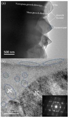
          We report a new method for growing hexagonal columnar nanograin structured silicon carbide (SiC) thin films on silicon substrates by using graphene–graphitic carbon nanoflakes (GGNs) templates from solid carbon sources. The growth was carried out in a conventional low pressure chemical vapor deposition system (LPCVD). The GGNs are small plates with lateral sizes of around 100 nm and overlap each other, and are made up of nanosized multilayer graphene and graphitic carbon matrix (GCM). Long and straight SiC nanograins with hexagonal shapes, and with lateral sizes of around 200–400 nm are synthesized on the GGNs, which form compact SiC thin films.

          Related collections

          Most cited references29

          • Record: found
          • Abstract: found
          • Article: found
          Is Open Access

          Electric Field Effect in Atomically Thin Carbon Films

          We report a naturally-occurring two-dimensional material (graphene that can be viewed as a gigantic flat fullerene molecule, describe its electronic properties and demonstrate all-metallic field-effect transistor, which uniquely exhibits ballistic transport at submicron distances even at room temperature.
            Bookmark
            • Record: found
            • Abstract: found
            • Article: found
            Is Open Access

            The Raman Fingerprint of Graphene

            Graphene is the two-dimensional (2d) building block for carbon allotropes of every other dimensionality. It can be stacked into 3d graphite, rolled into 1d nanotubes, or wrapped into 0d fullerenes. Its recent discovery in free state has finally provided the possibility to study experimentally its electronic and phonon properties. Here we show that graphene's electronic structure is uniquely captured in its Raman spectrum that clearly evolves with increasing number of layers. Raman fingerprints for single-, bi- and few-layer graphene reflect changes in the electronic structure and electron-phonon interactions and allow unambiguous, high-throughput, non-destructive identification of graphene layers, which is critically lacking in this emerging research area.
              Bookmark
              • Record: found
              • Abstract: not found
              • Article: not found

              Production of large‐area single‐crystal wafers of cubic SiC for semiconductor devices

                Bookmark

                Author and article information

                Journal
                Materials (Basel)
                Materials (Basel)
                materials
                Materials
                MDPI
                1996-1944
                16 April 2013
                April 2013
                : 6
                : 4
                : 1543-1553
                Affiliations
                [1 ]Key Laboratory of Semiconductor Materials Science, Institute of Semiconductors, Chinese Academy of Sciences, Beijing 100083, China; E-Mails: gshsun@ 123456red.semi.ac.cn (G.S.); liubin2010@ 123456semi.ac.cn (B.L.); ggyan@ 123456semi.ac.cn (G.Y.); guanmin@ 123456red.semi.ac.cn (M.G.); zhang_yang@ 123456mail.semi.ac.cn (Y.Z.); fzhang@ 123456semi.ac.cn (F.Z.); donglin09@ 123456semi.ac.cn (L.D.); liuero@ 123456semi.ac.cn (L.Z.); liushengbei@ 123456semi.ac.cn (S.L.); tianlixin@ 123456semi.ac.cn (L.T.); wangl@ 123456semi.ac.cn (L.W.); zwshuke@ 123456semi.ac.cn (W.Z.); ypzeng@ 123456red.semi.ac.cn (Y.Z.)
                [2 ]Semiconductor Lighting Technology Research and Development Center, Institute of Semiconductors, Chinese Academy of Sciences, Beijing 100083, China; E-Mail: chenyu@ 123456semi.ac.cn
                Author notes
                [* ]Author to whom correspondence should be addressed; E-Mails: liuxf@ 123456mail.semi.ac.cn (X.L.); chenyu@ 123456semi.ac.cn (Y.C.); Tel.: +86-10-8230-4101+86-10-8230-4783 (Y.C.); Fax: +86-10-8230-4232 (X.L. and Y.C.).
                Article
                materials-06-01543
                10.3390/ma6041543
                5452306
                8006067d-4ef8-4447-ad0a-35a4074c007d
                © 2013 by the authors.

                Licensee MDPI, Basel, Switzerland. This article is an open access article distributed under the terms and conditions of the Creative Commons Attribution license ( http://creativecommons.org/licenses/by/3.0/).

                History
                : 22 January 2013
                : 28 February 2013
                : 14 March 2013
                Categories
                Article

                hexagonal columnar,silicon carbide,thin film,graphene,nanoflake,solid carbon,cvd

                Comments

                Comment on this article