8
views
0
recommends
+1 Recommend
0 collections
    0
    shares
      • Record: found
      • Abstract: found
      • Article: found
      Is Open Access

      The Design and Life Test of a Multifunction Power Amplifier for Space Application

      Read this article at

      Bookmark
          There is no author summary for this article yet. Authors can add summaries to their articles on ScienceOpen to make them more accessible to a non-specialist audience.

          Abstract

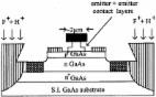
          A new multifunction power amplifier (MFPA) is designed and fabricated for the application of point-to-point K-Band backhaul TR module. A DC temperature life test was performed to model the up-limit temperature effect of the designed MFPA under space application. After 240 hours of 100°C life test, the test results illustrate that the designed MFPA has only slight power degradation at the saturation region without change of the linear gain. The general performance of the designed MFPA satisfies the requirement of the application scenario.

          Related collections

          Most cited references14

          • Record: found
          • Abstract: not found
          • Article: not found

          Breakdown walkout in pseudomorphic HEMT's

            Bookmark
            • Record: found
            • Abstract: found
            • Article: found
            Is Open Access

            Degradation Mechanisms for GaN and GaAs High Speed Transistors

            We present a review of reliability issues in AlGaN/GaN and AlGaAs/GaAs high electron mobility transistors (HEMTs) as well as Heterojunction Bipolar Transistors (HBTs) in the AlGaAs/GaAs materials systems. Because of the complex nature and multi-faceted operation modes of these devices, reliability studies must go beyond the typical Arrhenius accelerated life tests. We review the electric field driven degradation in devices with different gate metallization, device dimensions, electric field mitigation techniques (such as source field plate), and the effect of device fabrication processes for both DC and RF stress conditions. We summarize the degradation mechanisms that limit the lifetime of these devices. A variety of contact and surface degradation mechanisms have been reported, but differ in the two device technologies: For HEMTs, the layers are thin and relatively lightly doped compared to HBT structures and there is a metal Schottky gate that is directly on the semiconductor. By contrast, the HBT relies on pn junctions for current modulation and has only Ohmic contacts. This leads to different degradation mechanisms for the two types of devices.
              Bookmark
              • Record: found
              • Abstract: not found
              • Article: not found

              Reliability and degradation mechanism of AlGaAs/InGaAs and InAlAs/InGaAs HEMTs

                Bookmark

                Author and article information

                Journal
                Active and Passive Electronic Components
                Active and Passive Electronic Components
                Hindawi Limited
                0882-7516
                1563-5031
                2016
                2016
                : 2016
                :
                : 1-6
                Article
                10.1155/2016/1312721
                9fcde0e7-f1ee-4086-bd00-8e257189bf3e
                © 2016

                http://creativecommons.org/licenses/by/4.0/

                History

                Comments

                Comment on this article