8
views
0
recommends
+1 Recommend
0 collections
    0
    shares
      • Record: found
      • Abstract: found
      • Article: found
      Is Open Access

      Germanium epitaxy on silicon

      review-article

      Read this article at

      Bookmark
          There is no author summary for this article yet. Authors can add summaries to their articles on ScienceOpen to make them more accessible to a non-specialist audience.

          Abstract

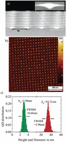
          With the rapid development of on-chip optical interconnects and optical computing in the past decade, silicon-based integrated devices for monolithic and hybrid optoelectronic integration have attracted wide attention. Due to its narrow pseudo-direct gap behavior and compatibility with Si technology, epitaxial Ge-on-Si has become a significant material for optoelectronic device applications. In this paper, we describe recent research progress on heteroepitaxy of Ge flat films and self-assembled Ge quantum dots on Si. For film growth, methods of strain modification and lattice mismatch relief are summarized, while for dot growth, key process parameters and their effects on the dot density, dot morphology and dot position are reviewed. The results indicate that epitaxial Ge-on-Si materials will play a bigger role in silicon photonics.

          Related collections

          Most cited references50

          • Record: found
          • Abstract: not found
          • Article: not found

          Dislocation-free Stranski-Krastanow growth of Ge on Si(100).

            Bookmark
            • Record: found
            • Abstract: not found
            • Article: not found

            High-performance Ge-on-Si photodetectors

              Bookmark
              • Record: found
              • Abstract: found
              • Article: not found

              An electrically pumped germanium laser.

              Electrically pumped lasing from Germanium-on-Silicon pnn heterojunction diode structures is demonstrated. Room temperature multimode laser with 1mW output power is measured. Phosphorous doping in Germanium at a concentration over 4x10 19 cm -3 is achieved. A Germanium gain spectrum of nearly 200nm is observed.
                Bookmark

                Author and article information

                Journal
                Sci Technol Adv Mater
                Sci Technol Adv Mater
                TSTA
                Science and Technology of Advanced Materials
                Taylor & Francis
                1468-6996
                1878-5514
                April 2014
                18 March 2014
                : 15
                : 2
                : 024601
                Affiliations
                [1 ]State Key Laboratory of Modern Optical Instrumentation, Department of Optical Engineering, Zhejiang University, Hangzhou, 310027, People’s Republic of China
                [2 ]State Key Laboratory on Integrated Optoelectronics, Institute of Semiconductors, Chinese Academy of Sciences, Beijing, 100083, People’s Republic of China
                Author notes
                Article
                TSTA11661152
                10.1088/1468-6996/15/2/024601
                5090408
                d69f80de-9bf7-458d-9ab4-da03c1ef88d6
                © 2014 National Institute for Materials Science

                Content from this work may be used under the terms of the Creative Commons Attribution-NonCommercial-ShareAlike 3.0 licence. Any further distribution of this work must maintain attribution to the author(s) and the title of the work, journal citation and DOI.

                History
                : 28 August 2013
                : 13 February 2014
                : 18 February 2014
                Categories
                Focus Articles

                epitaxial growth,germanium films,germanium quantum dots,strain modification,self assembly

                Comments

                Comment on this article