8
views
0
recommends
+1 Recommend
0 collections
    0
    shares
      • Record: found
      • Abstract: found
      • Article: not found

      Oriented Attachment and Nanorod Formation in Atomic Layer Deposition of TiO 2 on Graphene Nanoplatelets

      research-article

      Read this article at

      ScienceOpenPublisherPMC
      Bookmark
          There is no author summary for this article yet. Authors can add summaries to their articles on ScienceOpen to make them more accessible to a non-specialist audience.

          Abstract

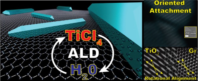
          Understanding the spontaneous organization of atoms on well-defined surfaces promises to enable control over the shape and size of supported nanostructures. Atomic layer deposition (ALD) boasts atomic-scale control in the synthesis of thin films and nanoparticles. Yet, the possibility to control the shape of ALD-grown nanostructures remains mostly unexplored. Here, we report on the bottom-up formation of both linear and V-shaped anatase TiO 2 nanorods (NRs) on graphene nanoplatelets during TiCl 4/H 2O ALD carried out at 300 °C. NRs as large as 200 nm form after only five ALD cycles, indicating that diffusional processes rather than layer-by-layer growth are behind the NR formation. In particular, high-resolution transmission electron microscopy reveals that the TiO 2 NRs and graphene nanoplatelets are in rotational alignment as a result of lattice matching. Crucially, we also show that individual nanocrystals can undergo in-plane oriented attachment.

          Related collections

          Most cited references58

          • Record: found
          • Abstract: not found
          • Article: not found

          Atomic layer deposition: an overview.

            Bookmark
            • Record: found
            • Abstract: not found
            • Article: not found

            Surface chemistry of atomic layer deposition: A case study for the trimethylaluminum/water process

              Bookmark
              • Record: found
              • Abstract: found
              • Article: not found

              Imperfect Oriented Attachment: Dislocation Generation in Defect-Free Nanocrystals

              Dislocations are common defects in solids, yet all crystals begin as dislocation-free nuclei. The mechanisms by which dislocations form during early growth are poorly understood. When nanocrystalline materials grow by oriented attachment at crystallographically specific surfaces and there is a small misorientation at the interface, dislocations result. Spiral growth at two or more closely spaced screw dislocations provides a mechanism for generating complex polytypic and polymorphic structures. These results are of fundamental importance to understanding crystal growth.
                Bookmark

                Author and article information

                Journal
                J Phys Chem C Nanomater Interfaces
                J Phys Chem C Nanomater Interfaces
                jy
                jpccck
                The Journal of Physical Chemistry. C, Nanomaterials and Interfaces
                American Chemical Society
                1932-7447
                1932-7455
                02 August 2018
                30 August 2018
                : 122
                : 34
                : 19981-19991
                Affiliations
                Department of Chemical Engineering, Delft University of Technology , 2629 HZ Delft, The Netherlands
                Author notes
                Article
                10.1021/acs.jpcc.8b05572
                6120748
                31b01e00-81e3-4024-8ddb-17a371211b69
                Copyright © 2018 American Chemical Society

                This is an open access article published under a Creative Commons Non-Commercial No Derivative Works (CC-BY-NC-ND) Attribution License, which permits copying and redistribution of the article, and creation of adaptations, all for non-commercial purposes.

                History
                : 11 June 2018
                : 01 August 2018
                Categories
                Article
                Custom metadata
                jp8b05572
                jp-2018-05572r

                Thin films & surfaces
                Thin films & surfaces

                Comments

                Comment on this article