26
views
0
recommends
+1 Recommend
0 collections
    0
    shares
      • Record: found
      • Abstract: found
      • Article: found
      Is Open Access

      Structural Investigation of Uniform Ensembles of Self-Catalyzed GaAs Nanowires Fabricated by a Lithography-Free Technique

      brief-report
      , ,
      Nanoscale Research Letters
      Springer US
      Nanowires, GaAs, Molecular beam epitaxy, Microstructure

      Read this article at

      Bookmark
          There is no author summary for this article yet. Authors can add summaries to their articles on ScienceOpen to make them more accessible to a non-specialist audience.

          Abstract

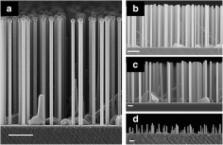
          Structural analysis of self-catalyzed GaAs nanowires (NWs) grown on lithography-free oxide patterns is described with insight on their growth kinetics. Statistical analysis of templates and NWs in different phases of the growth reveals extremely high-dimensional uniformity due to a combination of uniform nucleation sites, lack of secondary nucleation of NWs, and self-regulated growth under the effect of nucleation antibunching. Consequently, we observed the first evidence of sub-Poissonian GaAs NW length distributions. The high phase purity of the NWs is demonstrated using complementary transmission electron microscopy (TEM) and high-resolution X-ray diffractometry (HR-XRD). It is also shown that, while NWs are to a large extent defect-free with up to 2-μm-long twin-free zincblende segments, low-temperature micro-photoluminescence spectroscopy reveals that the proportion of structurally disordered sections can be detected from their spectral properties.

          Related collections

          Most cited references47

          • Record: found
          • Abstract: found
          • Article: not found

          InP nanowire array solar cells achieving 13.8% efficiency by exceeding the ray optics limit.

          Photovoltaics based on nanowire arrays could reduce cost and materials consumption compared with planar devices but have exhibited low efficiency of light absorption and carrier collection. We fabricated a variety of millimeter-sized arrays of p-type/intrinsic/n-type (p-i-n) doped InP nanowires and found that the nanowire diameter and the length of the top n-segment were critical for cell performance. Efficiencies up to 13.8% (comparable to the record planar InP cell) were achieved by using resonant light trapping in 180-nanometer-diameter nanowires that only covered 12% of the surface. The share of sunlight converted into photocurrent (71%) was six times the limit in a simple ray optics description. Furthermore, the highest open-circuit voltage of 0.906 volt exceeds that of its planar counterpart, despite about 30 times higher surface-to-volume ratio of the nanowire cell.
            Bookmark
            • Record: found
            • Abstract: not found
            • Article: not found

            Critical dimensions for the plastic relaxation of strained axial heterostructures in free-standing nanowires

            Frank Glas (2006)
              Bookmark
              • Record: found
              • Abstract: found
              • Article: not found

              A III-V nanowire channel on silicon for high-performance vertical transistors.

              Silicon transistors are expected to have new gate architectures, channel materials and switching mechanisms in ten years' time. The trend in transistor scaling has already led to a change in gate structure from two dimensions to three, used in fin field-effect transistors, to avoid problems inherent in miniaturization such as high off-state leakage current and the short-channel effect. At present, planar and fin architectures using III-V materials, specifically InGaAs, are being explored as alternative fast channels on silicon because of their high electron mobility and high-quality interface with gate dielectrics. The idea of surrounding-gate transistors, in which the gate is wrapped around a nanowire channel to provide the best possible electrostatic gate control, using InGaAs channels on silicon, however, has been less well investigated because of difficulties in integrating free-standing InGaAs nanostructures on silicon. Here we report the position-controlled growth of vertical InGaAs nanowires on silicon without any buffering technique and demonstrate surrounding-gate transistors using InGaAs nanowires and InGaAs/InP/InAlAs/InGaAs core-multishell nanowires as channels. Surrounding-gate transistors using core-multishell nanowire channels with a six-sided, high-electron-mobility transistor structure greatly enhance the on-state current and transconductance while keeping good gate controllability. These devices provide a route to making vertically oriented transistors for the next generation of field-effect transistors and may be useful as building blocks for wireless networks on silicon platforms.
                Bookmark

                Author and article information

                Contributors
                eero.koivusalo@tut.fi
                Journal
                Nanoscale Res Lett
                Nanoscale Res Lett
                Nanoscale Research Letters
                Springer US (New York )
                1931-7573
                1556-276X
                16 March 2017
                16 March 2017
                2017
                : 12
                : 192
                Affiliations
                ISNI 0000 0000 9327 9856, GRID grid.6986.1, Optoelectronics Research Centre, , Tampere University of Technology, ; Korkeakoulunkatu 3, FI-33720 Tampere, Finland
                Author information
                http://orcid.org/0000-0001-5029-4658
                Article
                1989
                10.1186/s11671-017-1989-9
                5355414
                28314359
                7cff36e9-8883-4972-ac98-23fac301d4ae
                © The Author(s). 2017

                Open AccessThis article is distributed under the terms of the Creative Commons Attribution 4.0 International License ( http://creativecommons.org/licenses/by/4.0/), which permits unrestricted use, distribution, and reproduction in any medium, provided you give appropriate credit to the original author(s) and the source, provide a link to the Creative Commons license, and indicate if changes were made.

                History
                : 17 January 2017
                : 9 March 2017
                Funding
                Funded by: FundRef http://dx.doi.org/10.13039/501100005877, Luonnontieteiden ja Tekniikan Tutkimuksen Toimikunta;
                Award ID: 294630
                Award Recipient :
                Categories
                Nano Express
                Custom metadata
                © The Author(s) 2017

                Nanomaterials
                nanowires,gaas,molecular beam epitaxy,microstructure
                Nanomaterials
                nanowires, gaas, molecular beam epitaxy, microstructure

                Comments

                Comment on this article