8
views
0
recommends
+1 Recommend
0 collections
    0
    shares
      • Record: found
      • Abstract: found
      • Article: found
      Is Open Access

      Subwavelength pixelated CMOS color sensors based on anti-Hermitian metasurface

      research-article

      Read this article at

      Bookmark
          There is no author summary for this article yet. Authors can add summaries to their articles on ScienceOpen to make them more accessible to a non-specialist audience.

          Abstract

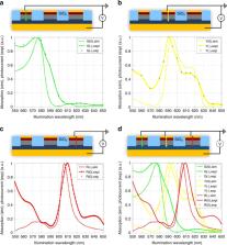
          The demand for essential pixel components with ever-decreasing size and enhanced performance is central to current optoelectronic applications, including imaging, sensing, photovoltaics and communications. The size of the pixels, however, are severely limited by the fundamental constraints of lightwave diffraction. Current development using transmissive filters and planar absorbing layers can shrink the pixel size, yet there are two major issues, optical and electrical crosstalk, that need to be addressed when the pixel dimension approaches wavelength scale. All these fundamental constraints preclude the continual reduction of pixel dimensions and enhanced performance. Here we demonstrate subwavelength scale color pixels in a CMOS compatible platform based on anti-Hermitian metasurfaces. In stark contrast to conventional pixels, spectral filtering is achieved through structural color rather than transmissive filters leading to simultaneously high color purity and quantum efficiency. As a result, this subwavelength anti-Hermitian metasurface sensor, over 28,000 pixels, is able to sort three colors over a 100 nm bandwidth in the visible regime, independently of the polarization of normally-incident light. Furthermore, the quantum yield approaches that of commercial silicon photodiodes, with a responsivity exceeding 0.25 A/W for each channel. Our demonstration opens a new door to sub-wavelength pixelated CMOS sensors and promises future high-performance optoelectronic systems.

          Abstract

          Pixel size in imaging and displays is limited by fundamental constraints that compromise performance at wavelength scales. Here the authors present subwavelength color pixel sensors based on anti-Hermitian metasurfaces relying on structural color for increased performance.

          Related collections

          Most cited references19

          • Record: found
          • Abstract: not found
          • Article: not found

          Subwavelength-thick lenses with high numerical apertures and large efficiency based on high-contrast transmitarrays

            Bookmark
            • Record: found
            • Abstract: found
            • Article: not found

            Designing dielectric resonators on substrates: combining magnetic and electric resonances.

            High-performance integrated optics, solar cells, and sensors require nanoscale optical components at the surface of the device, in order to manipulate, redirect and concentrate light. High-index dielectric resonators provide the possibility to do this efficiently with low absorption losses. The resonances supported by dielectric resonators are both magnetic and electric in nature. Combined scattering from these two can be used for directional scattering. Most applications require strong coupling between the particles and the substrate in order to enhance the absorption in the substrate. However, the coupling with the substrate strongly influences the resonant behavior of the particles. Here, we systematically study the influence of particle geometry and dielectric environment on the resonant behavior of dielectric resonators in the visible to near-IR spectral range. We show the key role of retardation in the excitation of the magnetic dipole (MD) mode, as well as the limit where no MD mode is supported. Furthermore, we study the influence of particle diameter, shape and substrate index on the spectral position, width and overlap of the electric dipole (ED) and MD modes. Also, we show that the ED and MD mode can selectively be enhanced or suppressed using multi-layer substrates. And, by comparing dipole excitation and plane wave excitation, we study the influence of driving field on the scattering properties. Finally, we show that the directional radiation profiles of the ED and MD modes in resonators on a substrate are similar to those of point-dipoles close to a substrate. Altogether, this work is a guideline how to tune magnetic and electric resonances for specific applications.
              Bookmark
              • Record: found
              • Abstract: found
              • Article: not found

              Filter-free image sensor pixels comprising silicon nanowires with selective color absorption.

              The organic dye filters of conventional color image sensors achieve the red/green/blue response needed for color imaging, but have disadvantages related to durability, low absorption coefficient, and fabrication complexity. Here, we report a new paradigm for color imaging based on all-silicon nanowire devices and no filters. We fabricate pixels consisting of vertical silicon nanowires with integrated photodetectors, demonstrate that their spectral sensitivities are governed by nanowire radius, and perform color imaging. Our approach is conceptually different from filter-based methods, as absorbed light is converted to photocurrent, ultimately presenting the opportunity for very high photon efficiency.
                Bookmark

                Author and article information

                Contributors
                xiang@berkeley.edu
                Journal
                Nat Commun
                Nat Commun
                Nature Communications
                Nature Publishing Group UK (London )
                2041-1723
                6 August 2020
                6 August 2020
                2020
                : 11
                : 3916
                Affiliations
                [1 ]GRID grid.47840.3f, ISNI 0000 0001 2181 7878, Nano-Scale Science and Engineering Center (NSEC), 3112 Etcheverry Hall, University of California Berkeley, ; Berkeley, CA 94720 USA
                [2 ]GRID grid.419666.a, ISNI 0000 0001 1945 5898, Samsung Advanced Institute of Technology, Samsung Electronics Co. Ltd., Samsung-ro 130, Yeongtong-gu, Suwon-si, ; Gyeonggi-do, 16678 Korea
                [3 ]GRID grid.194645.b, ISNI 0000000121742757, Faculties of Sciences and Engineering, , University of Hong Kong, ; Hong Kong, China
                Author information
                http://orcid.org/0000-0002-9193-7805
                http://orcid.org/0000-0003-0151-791X
                http://orcid.org/0000-0002-3272-894X
                Article
                17743
                10.1038/s41467-020-17743-y
                7413260
                32764547
                e5f9e9fd-6e77-46c4-9607-af63203c6c5c
                © The Author(s) 2020

                Open Access This article is licensed under a Creative Commons Attribution 4.0 International License, which permits use, sharing, adaptation, distribution and reproduction in any medium or format, as long as you give appropriate credit to the original author(s) and the source, provide a link to the Creative Commons license, and indicate if changes were made. The images or other third party material in this article are included in the article’s Creative Commons license, unless indicated otherwise in a credit line to the material. If material is not included in the article’s Creative Commons license and your intended use is not permitted by statutory regulation or exceeds the permitted use, you will need to obtain permission directly from the copyright holder. To view a copy of this license, visit http://creativecommons.org/licenses/by/4.0/.

                History
                : 18 December 2019
                : 14 July 2020
                Funding
                Funded by: FundRef https://doi.org/10.13039/100004358, Samsung;
                Categories
                Article
                Custom metadata
                © The Author(s) 2020

                Uncategorized
                optoelectronic devices and components,sub-wavelength optics,imaging and sensing

                Comments

                Comment on this article